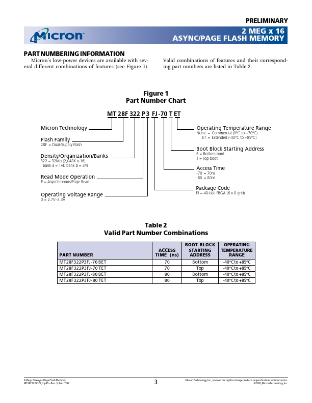
MT28F322P3 Overview
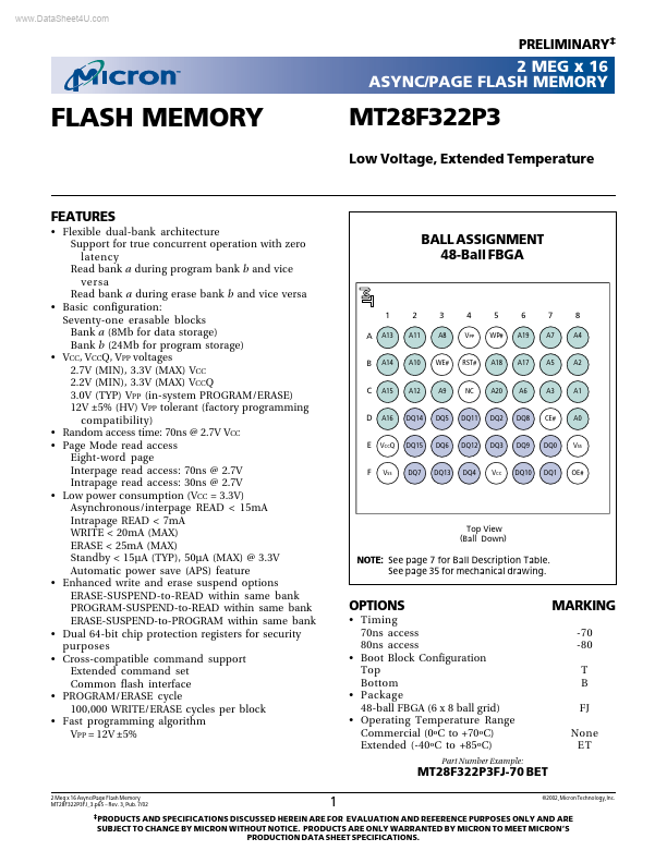
See page 35 for mechanical drawing. OPTIONS Timing 70ns access 80ns access Boot Block Configuration Top Bottom Package 48-ball FBGA (6 x 8 ball grid) Operating Temperature Range mercial (0ºC to +70ºC) Extended (-40ºC to +85ºC) Part Number Example: 7/02 1 ©2002, Micron Technology, Inc.
MT28F322P3 Key Features
- Flexible dual-bank architecture Support for true concurrent operation with zero latency Read bank a during program bank
- Basic configuration: Seventy-one erasable blocks Bank a (8Mb for data storage) Bank b (24Mb for program storage)
- VCC, VCCQ, VPP voltages 2.7V (MIN), 3.3V (MAX) VCC 2.2V (MIN), 3.3V (MAX) VCCQ 3.0V (TYP) VPP (in-system PROGRAM/ERASE)
- Random access time: 70ns @ 2.7V VCC
- Page Mode read access Eight-word page Interpage read access: 70ns @ 2.7V Intrapage read access: 30ns @ 2.7V
- Low power consumption (VCC = 3.3V) Asynchronous/interpage READ < 15mA Intrapage READ < 7mA WRITE < 20mA (MAX) ERASE < 25
- Enhanced write and erase suspend options ERASE-SUSPEND-to-READ within same bank PROGRAM-SUSPEND-to-READ within same bank
- Dual 64-bit chip protection registers for security purposes
- Cross-patible mand support Extended mand set mon flash interface
- PROGRAM/ERASE cycle 100,000 WRITE/ERASE cycles per block