Datasheet Summary
TECHNICAL DATA
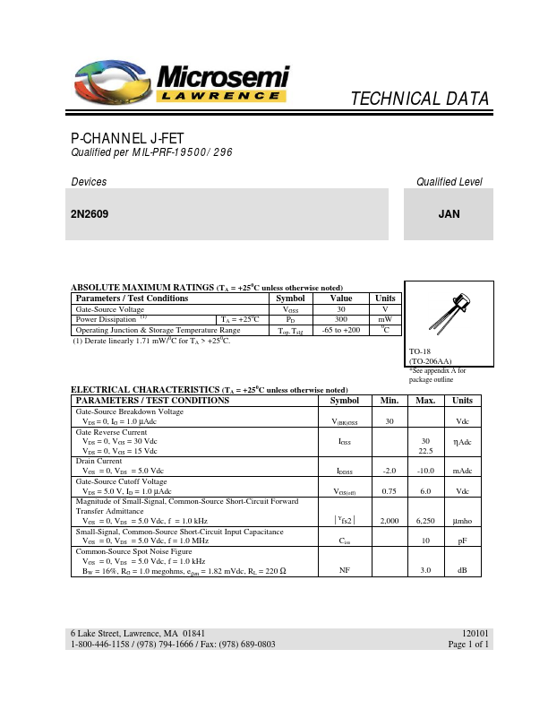
P-CHANNEL J-FET
Qualified per MIL-PRF-19500/296 Devices 2N2609 Qualified Level...
| Manufacturer | Part Number | Description |
|---|---|---|
| NES NES |
2N2609 | P-CHANNEL POWER MOSFET |
| 2N2609 | P-Channel JFET | |
| 2N2609 | GENERAL PURPOSE JFET |