XD1002-BD Overview
Description
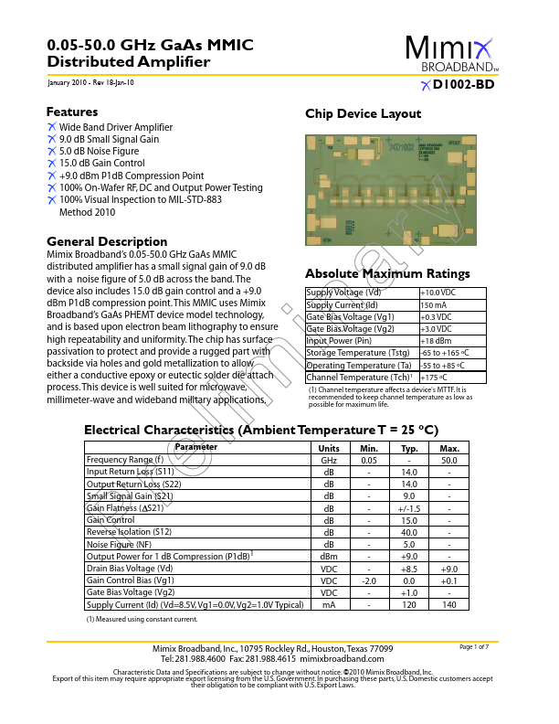
Mimix Broadband’s 0.05-50.0 GHz GaAs MMIC distributed amplifier has a small signal gain of 9.0 dB with a noise figure of 5.0 dB across the device also includes 15.0 dB gain control and a +9.0 dBm P1dB compression MMIC uses Mimix Broadband’s GaAs PHEMT device model technology, and is based upon electron beam lithography to ensure high repeatability and chip has surface passivation to protect and provide a rugged part with backside via holes and gold metallization to allow either a conductive epoxy or eutectic solder die attach device is well suited for microwave, millimeter-wave and wideband military applications. Supply Voltage (Vd) +10.0 VDC Supply Current (Id) 150 mA Gate Bias Voltage (Vg1) +0.3 VDC Gate Bias Voltage (Vg2) +3.0 VDC Input Power (Pin) +18 dBm Storage Temperature (Tstg) -65 to +165 ºC Operating Temperature (Ta) -55 to +85 ºC Channel Temperature (Tch)1 +175 ºC (1) Channel temperature affects a device's MTTF.