Datasheet Summary
8.5-11.0 GHz GaAs Power Amplifier Flange, 10 pin
August 2006
- Rev 16-Aug-06
P1006-FA Features
X-Band 10W Power Amplifier Flange Package 21.5 dB Large Signal Gain +40.5 dBm Saturated Output Power 37% Power Added Efficiency 100% On-Wafer RF, DC and Output Power Testing
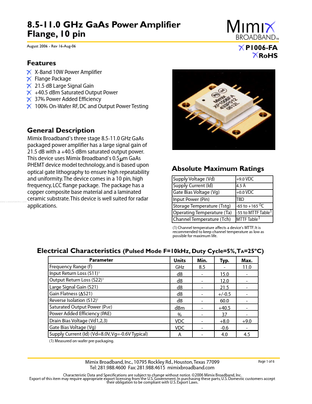
Mimix Broadband’s three stage 8.5-11.0 GHz GaAs packaged power amplifier has a large signal gain of 21.5 dB with a +40.5 dBm saturated output power. This device uses Mimix Broadband’s 0.5 m GaAs PHEMT device model technology, and is based upon optical gate lithography to ensure high repeatability and uniformity. The device es in a 10 pin, high frequency, LCC flange package. The package has a copper posite base...