XP1006
XP1006 is GaAs MMIC Power Amplifier manufactured by Mimix Broadband.
Features
X-Band 10W Power Amplifier 21.0 d B Large Signal Gain +40.0 d Bm Saturated Output Power 30% Power Added Efficiency On-chip Gate Bias Circuit 100% On-Wafer RF, DC and Output Power Testing 100% Visual Inspection to MIL-STD-883 Method 2010 Mimix Broadband’s three stage 8.5-11.0 GHz Ga As MMIC power amplifier has a large signal gain of 21.0 d B with a +40.0 d Bm saturated output power and also includes on-chip gate bias circuitry. This MMIC uses Mimix Broadband’s 0.5 m Ga As PHEMT device model technology, and is based upon optical gate lithography to ensure high repeatability and uniformity. The chip has surface passivation to protect and provide a rugged part with backside via holes and gold metallization to allow either a conductive .. epoxy or eutectic solder die attach process. This device is well suited for radar applications.
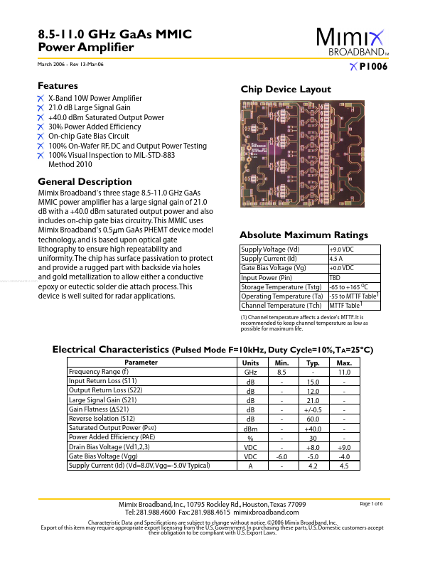
Chip Device Layout
XP1006 MIMIX BROADBAND 10004966 TNO COPYRIGHT 2005 X=4940 Y=4290
General Description
Absolute Maximum Ratings
Supply Voltage (Vd) Supply Current (Id) Gate Bias Voltage (Vg) Input Power (Pin) Storage Temperature (Tstg) Operating Temperature (Ta) Channel Temperature (Tch)
+9.0 VDC 4.5 A +0.0 VDC TBD -65 to +165 OC -55 to MTTF Table1 MTTF Table 1
(1) Channel temperature affects a device's MTTF. It is remended to keep channel temperature as low as possible for maximum life.
Electrical Characteristics (Pulsed Mode F=10k Hz, Duty Cycle=10%,TA=25ºC)
Parameter Frequency Range (f ) Input Return Loss (S11) Output Return Loss (S22) Large Signal Gain (S21) Gain Flatness ( S21) Reverse Isolation (S12) Saturated Output Power (PSAT) Power Added Efficiency (PAE) Drain Bias Voltage (Vd1,2,3) Gate Bias Voltage (Vgg) Supply Current (Id) (Vd=8.0V, Vgg=-5.0V Typical) Units GHz d B d B d B d B d B d Bm % VDC VDC A Min. 8.5 -6.0 Typ. 15.0 12.0 21.0 +/-0.5 60.0 +40.0 30 +8.0 -5.0 4.2 Max. 11.0 +9.0 -4.0 4.5
Mimix Broadband, Inc., 10795 Rockley Rd., Houston, Texas 77099 Tel: 281.988.4600 Fax: 281.988.4615 mimixbroadband.
Page 1 of...