Datasheet4U Logo Datasheet4U.com

XP1017 - GaAs MMIC Power Amplifier

Datasheet Summary

Description

Absolute Maximum Ratings Supply Voltage (Vd) Supply Current (Id) Gate Bias Voltage Input Power (Pin) Storage Temperature (Tstg) Operating Temperature (Ta) Channel Temperature (Tch) +6.0 VDC 950 mA +0.3 VDC +15 dBm -65 to +165 OC -55 to MTTF TAble4 MTTF Table 4 (4) Channel temperature affects a dev

Features

  • Balanced Design Provides Good Input/Output Match On-Chip Temperature Compensated Output Power Detector 16.0 dB Small Signal Gain +33.0 dBm Third Order Intercept (OIP3) 100% On-Wafer RF, DC and Output Power Testing 100% Visual Inspection to MIL-STD-883 Method 2010 Mimix Broadband’s two stage 30.0-36.0 GHz GaAs MMIC power amplifier is optimized for linear operation with a third order intercept point of +33.0 dBm. The device also includes Lange couplers to achieve good input/output return loss and.

📥 Download Datasheet

Datasheet preview – XP1017

Datasheet Details

Part number XP1017
Manufacturer Mimix Broadband
File Size 277.69 KB
Description GaAs MMIC Power Amplifier
Datasheet download datasheet XP1017 Datasheet
Additional preview pages of the XP1017 datasheet.
Other Datasheets by Mimix Broadband

Full PDF Text Transcription

Click to expand full text
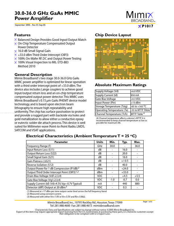
30.0-36.0 GHz GaAs MMIC Power Amplifier September 2005 - Rev 01-Sep-05 P1017 Chip Device Layout Features Balanced Design Provides Good Input/Output Match On-Chip Temperature Compensated Output Power Detector 16.0 dB Small Signal Gain +33.0 dBm Third Order Intercept (OIP3) 100% On-Wafer RF, DC and Output Power Testing 100% Visual Inspection to MIL-STD-883 Method 2010 Mimix Broadband’s two stage 30.0-36.0 GHz GaAs MMIC power amplifier is optimized for linear operation with a third order intercept point of +33.0 dBm. The device also includes Lange couplers to achieve good input/output return loss and an on-chip temperature compensated output power detector. This MMIC uses Mimix Broadband’s 0.
Published: |