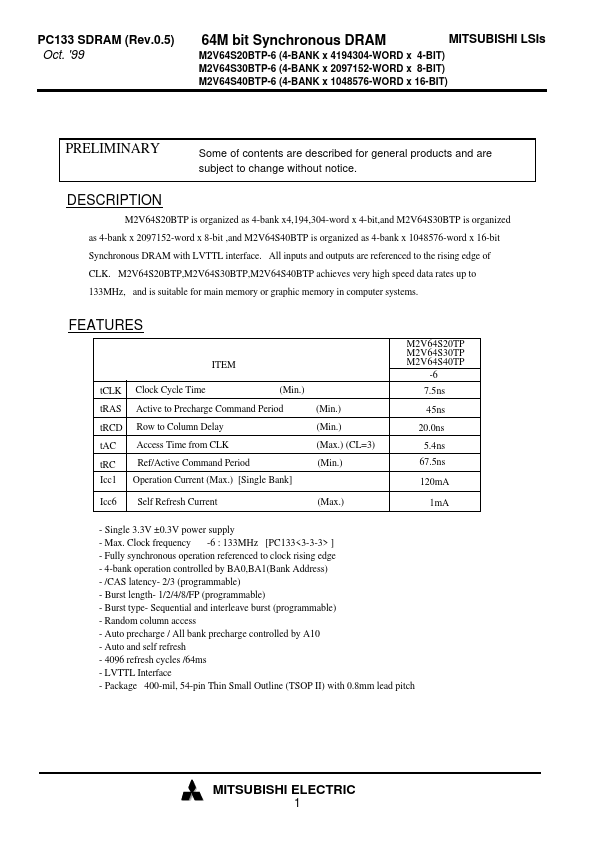
M2V64S20TP
DESCRIPTION
M2V64S20BTP is organized as 4-bank x4,194,304-word x 4-bit,and M2V64S30BTP is organized as 4-bank x 2097152-word x 8-bit ,and M2V64S40BTP is organized as 4-bank x 1048576-word x 16-bit Synchronous DRAM with LVTTL interface. All inputs and outputs are referenced to the rising edge of CLK. M2V64S20BTP,M2V64S30BTP,M2V64S40BTP achieves very high speed data rates up to 133MHz, and is suitable for main memory or graphic memory in puter systems.
FEATURES
ITEM t CLK t RAS t RCD t AC t RC Icc1 Icc6 Clock Cycle Time (Min.) (Min.) (Min.) (Max.) (CL=3) (Min.) M2V64S20TP M2V64S30TP M2V64S40TP -6 7.5ns 45ns 20.0ns 5.4ns 67.5ns 120m A (Max.) 1m A
Active to Precharge mand Period Row to Column Delay Access Time from CLK Ref/Active mand Period Operation Current (Max.) [Single Bank] Self Refresh Current
- Single 3.3V ±0.3V power supply
- Max. Clock frequency -6 : 133MHz [PC133<3-3-3> ]
- Fully synchronous operation referenced to clock rising edge
- 4-bank operation controlled by BA0,BA1(Bank...