M5M4V4S40CTP-15
M5M4V4S40CTP-15 is 4M (2-BANK x 131072-WORD x 16-BIT) Synchronous DRAM manufactured by Mitsubishi Electric.
- Part of the M5M comparator family.
- Part of the M5M comparator family.
SDRAM (Rev. 0.3)
MITSUBISHI LSIs
Feb ‘97 Preliminary
M5M4V4S40CTP-12, -15
4M (2-BANK x 131072-WORD x 16-BIT) Synchronous DRAM
PRELIMINARY
Some of contents are described for general products and are subject to change without notice.
DESCRIPTION
The M5M4V4S40CTP is a 2-bank x 131,072-word x 16-bit Synchronous DRAM, with LVTTL interface. All inputs and outputs are referenced to the rising edge of CLK. The M5M4V4S40CTP achieves very high speed data rates up to 83MHz, and is suitable for main memory or graphic memory in puter systems.
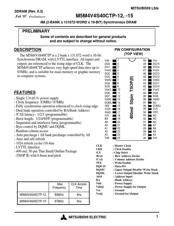
Vdd DQ0 DQ1 Vss Q DQ2 DQ3 Vdd Q DQ4 DQ5 Vss Q DQ6 DQ7 Vdd Q DQML /WE /CAS /RAS /CS BA A8 A0 A1 A2 A3 Vdd
PIN CONFIGURATION (TOP VIEW)
1 2 3 4 5 6 7 8 9 10 11 12 13 14 15 16 17 18 19 20 21 22 23 24 25 50 49 48 47 46 45 44 43 42 41 40 39 38 37 36 35 34 33 32 31 30 29 28 27 26 Vss DQ15 DQ14 Vss Q DQ13 DQ12 Vdd Q DQ11 DQ10 Vss Q DQ9 DQ8 Vdd Q NC DQMU CLK CKE NC NC NC A7 A6 A5 A4 Vss
Features
- Single 3.3v±0.3v power supply
- Clock frequency 83MHz / 67MHz
- Fully synchronous operation referenced to clock rising edge
- Dual bank operation controlled by BA(Bank Address)
- /CAS latency- 1/2/3 (programmable)
- Burst length- 1/2/4/8/FP (programmable)
- Sequential and interleave burst (programmable)
- Byte control by DQMU and DQML
- Random column access
- Auto precharge / All bank precharge controlled by A8
- Auto and self refresh
- 1024 refresh cycles /16.4ms CLK
- LVTTL Interface CKE
- 400-mil, 50-pin Thin Small Outline Package /CS (TSOP II) with 0.8mm lead pitch /RAS
Max. Frequency M5M4V4S40CTP-12 M5M4V4S40CTP-15 83MHz 67MHz
CLK Access Time 8ns 9ns
/CAS /WE DQ0-15 DQMU DQML A0-8 BA Vdd Vdd Q Vss Vss...