2N5555
Description
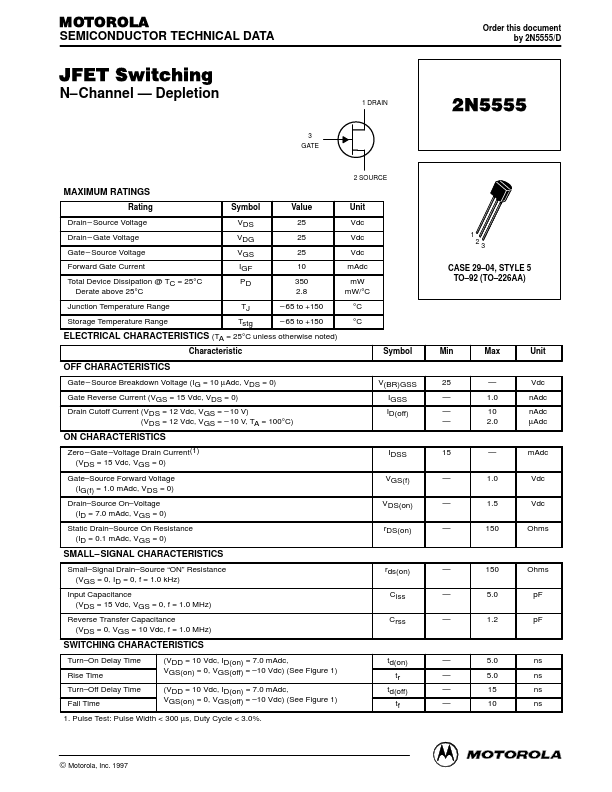
MOTOROLA SEMICONDUCTOR TECHNICAL DATA Order this document by 2N5555/D JFET Switching N–Channel — Depletion 3 GATE 1 DRAIN 2N5555 2 SOURCE MAXIMUM RATINGS Rating Drain – Source Voltage Drain – ...
MOTOROLA SEMICONDUCTOR TECHNICAL DATA Order this document by 2N5555/D JFET Switching N–Channel — Depletion 3 GATE 1 DRAIN 2N5555 2 SOURCE MAXIMUM RATINGS Rating Drain – Source Voltage Drain – ...