VN2406L
Description
MOTOROLA SEMICONDUCTOR TECHNICAL DATA Order this document by VN2406L/D TMOS FET Transistor N–Channel — Enhancement 3 DRAIN 2 GATE VN2406L Motorola Preferred Device 1 SOURCE MAXIMUM RATINGS Rati...
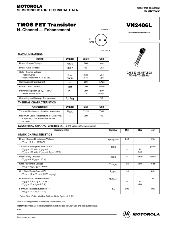
MOTOROLA SEMICONDUCTOR TECHNICAL DATA Order this document by VN2406L/D TMOS FET Transistor N–Channel — Enhancement 3 DRAIN 2 GATE VN2406L Motorola Preferred Device 1 SOURCE MAXIMUM RATINGS Rati...
| Part Number | Manufacturer | Description |
|---|---|---|
| VN2406L | Siliconix | N-Channel Enhancement-Mode MOS Transistors |
| VN2406L | onsemi | Small Signal MOSFET |
| VN2406L | Vishay | N-Channel MOSFETs |
| VN2406D | Vishay | N-Channel MOSFETs |
| VN2406 | Supertex Inc | N-Channel Vertical DMOS FETs |
| VN2406B | Siliconix | N-Channel Enhancement-Mode MOS Transistors |
| VN2406D | Siliconix | N-Channel Enhancement-Mode MOS Transistors |