Datasheet Summary
Freescale Semiconductor, Inc.
Advance Information
MPC8240EC Rev. 4, 11/2003 MPC8240 Integrated Processor Hardware Specifications
Freescale Semiconductor, Inc...
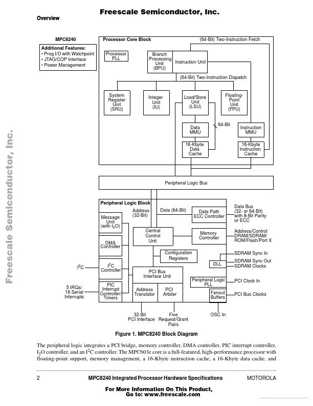
The MPC8240 bines a MPC603e core microprocessor with a PCI bridge. The MPC8240 PCI support allows system designers to rapidly create systems using peripherals already designed for PCI and the other standard interfaces. The MPC8240 also integrates a high-performance memory controller that supports various types of DRAM and ROM. The MPC8240 is the first of a family of products that provide system-level support for industry standard interfaces with PowerPC™ microprocessor cores. This hardware specification describes pertinent...