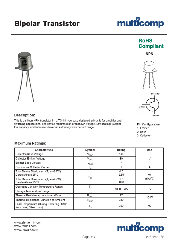
DESCRIPTION
: MAXIMUM RATINGS
: Characteristic Collector-Base Voltage Collector-Emitter Voltage Emitter Base Voltage Continuous Collector Current Total Device Dissipation -(TA = +25°C), Derate Above 25°C Total Device Dissipation -(TA = +25°C), Derate Above 25°C Operating Junction Temperature Range Storage Temperature Range, Thermal Resistance, Junction-to-Case Thermal Resistance, Junction-to-Ambient Lead Temperature (During Soldering, 1/16" from case, 60sec max) Symbol VCBO VCEO VEBO IC PD TJ Tstg RthJC RthJA TL Rating 140 80 7 1 0.5 2.85 1.8 10.6 -65 to +200 97 350 300 Pin Configuration: 1. Emitter 2. Base 3. Collector Unit V A W mW/°C °C °C/W °C Page <1> Multicomp