2SJ599
2SJ599 is P-Channel MOSFET manufactured by NEC.
DESCRIPTION
The 2SJ599 is P-channel MOS Field Effect Transistor designed for solenoid, motor and lamp driver. ..
ORDERING INFORMATION
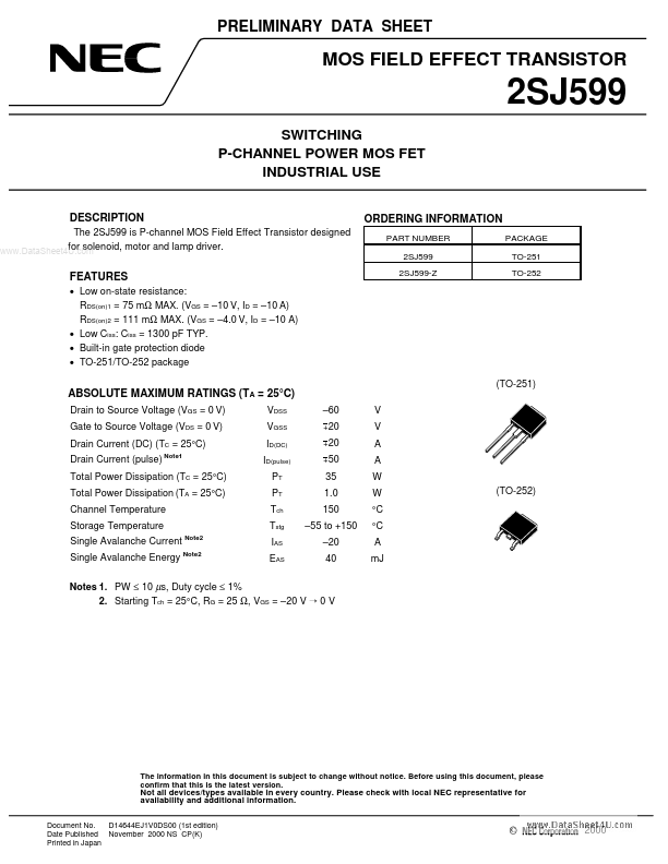
PART NUMBER 2SJ599 2SJ599-Z PACKAGE TO-251 TO-252
FEATURES
- Low on-state resistance: RDS(on)1 = 75 mΩ MAX. (VGS =
- 10 V, ID =
- 10 A) RDS(on)2 = 111 mΩ MAX. (VGS =
- 4.0 V, ID =
- 10 A)
- Low Ciss: Ciss = 1300 p F TYP.
- Built-in gate protection diode
- TO-251/TO-252 package
ABSOLUTE MAXIMUM RATINGS (TA = 25°C)
Drain to Source Voltage (VGS = 0 V) Gate to Source Voltage (VDS = 0 V) Drain Current (DC) (TC = 25°C) Drain Current (pulse)
Note1
(TO-251)
- 60
+ 20 + 20 + 50
VDSS VGSS ID(DC) ID(pulse) PT PT Tch Tstg
V V A A W W °C °C A m J (TO-252)
Total Power Dissipation (TC = 25°C) Total Power Dissipation (TA = 25°C) Channel Temperature Storage Temperature Single Avalanche Current Single Avalanche Energy
Note2 Note2
35 1.0 150
- 55 to +150
- 20 40
IAS EAS
Notes 1. PW ≤ 10 µs, Duty cycle ≤ 1% 2. Starting Tch = 25°C, RG = 25 Ω, VGS =
- 20 V ¡ 0 V
The information in this document is subject to change without notice. Before using this document, please confirm that this is the latest version.
Not all devices/types available in every country. Please check with local NEC representative for availability and additional information.
Document No. D14644EJ1V0DS00 (1st edition) Date Published November 2000 NS CP(K) Printed in Japan
©
ELECTRICAL CHARACTERISTICS (TA = 25°C)
CHARACTERISTICS Zero Gate Voltage Drain Current Gate Leakage Current Gate Cut-off Voltage Forward Transfer Admittance Drain to Source On-state Resistance SYMBOL IDSS IGSS VGS(off) | yfs | RDS(on)1 RDS(on)2 Input Capacitance
.. Output Capacitance
TEST CONDITIONS VDS =
- 60 V, VGS = 0 V VGS = + 20 V, VDS = 0 V VDS =
- 10 V, ID =
- 1 m A VDS...