2SK2158
2SK2158 is N-CHANNEL MOS FET manufactured by NEC.
FEATURES
- Capable of drive gate with 1.5 V
- Because of high input impedance, there is no need to consider driving current.
- Bias resistance can be omitted, enabling reduction in total number of parts.
0.95 0.95
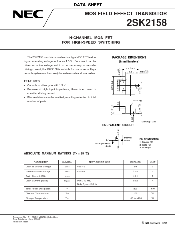
+0.1 +0.1
Marking
1.1 to 1.4
0 to 0.1
- 0.06
Marking: G23 PIN CONNECTION 1. Source (S) 2. Gate (G) 3. Drain (D)
EQUIVALENT CIRCUIT
3 Internal diode
2 Gate protection diode 1
ABSOLUTE MAXIMUM RATINGS (TA = 25 ˚C)
PARAMETER Drain to Source Voltage Gate to Source Voltage Drain Current (DC) Drain Current (pulse) SYMBOL VDSS VGSS ID(DC) ID(pulse) PW ≤ 10 ms, Duty Cycle ≤ 50 % VGS = 0 VDS = 0 TEST CONDITIONS RATINGS 50 ± 7.0 ± 0.1 ± 0.2 UNIT V V A A
Total Power Dissipation Channel Temperature Storage Temperature
PT Tch Tstg
200 150
- 55 to +150
- 0.05
3 m W ˚C ˚C
Document No. D11234EJ1V0DS00 (1st edition) Date Published June 1996 P Printed in Japan
©
ELECTRICAL CHARACTERISTICS (TA = 25 ˚C)
PARAMETER Drain Cut-off Current Gate Leakage Current Gate Cut-off Voltage Forward Transfer Admittance Drain to Source On-state Resistance Drain to Source On-state Resistance Drain to Source On-state Resistance Input Capacitance Output Capacitance Reverse Transfer Capacitance Turn-On Delay Time Rise Time Turn-Off Delay Time Fall Time SYMBOL IDSS IGSS VGS(off) | yfs | RDS(on)1 RDS(on)2 RDS(on)3 Ciss Coss Crss td(on) tr td(off) tf VDD = 3 V, ID = 20 m A VGS(on) = 3 V, RG = 10 Ω RL = 150 Ω TEST CONDITIONS VDS = 50 V, VGS = 0 VGS = ± 7.0 V, VDS = 0 VDS = 3 V, ID = 1.0 µA VDS = 3 V, ID = 10 m A VGS = 1.5 V, ID = 1.0 m A VGS = 2.5 V, ID = 10 m A VGS = 4.0 V, ID = 10 m A VDS = 3 V, VGS = 0 f = 1.0 MHz 0.5 20 32 16 12 6 8 1 9 48 21 31 50 20 15 0.7 MIN. TYP. MAX. 1.0 ± 3.0 1.1 UNIT
µA µA
V m S Ω Ω Ω p F p F p F ns ns ns ns
TYPICAL CHARACTERISTICS (TA = 25 ˚C)
DERATING FACTOR OF FORWARD BIAS SAFE OPERATING AREA 100 200
V 7 d T
- Derating Factor
- % ID
- Drain Current
- m...