Datasheet4U Logo Datasheet4U.com

UPA1730 - P-Channel Power MOSFET

Datasheet Summary

Description

The µ PA1730 is P-Channel MOS Field Effect Transistor designed for power management applications of notebook computers and Li-ion battery protection circuit.

Features

  • Low on-resistance 1.44 RDS(on)1 = 9.5 mΩ MAX. (VGS =.
  • 10 V, ID =.
  • 6.5 A) 1.8 MAX. 1 5.37 MAX. 4 6.0 ±0.3 4.4 +0.10.
  • 0.05 RDS(on)2 = 13.5 mΩ MAX. (VGS =.
  • 4.5 V, ID =.
  • 6.5 A) 5 RDS(on)3 = 15.0 mΩ MAX. (VGS =.
  • 4.0 V, ID =.
  • 6.5 A).
  • Low Ciss : Ciss = 3800 pF TYP.
  • Built-in G-S protection diode.
  • Small and surface mount package (Power SOP8) 0.8 0.15 0.05 MIN. 0.5 ±0.2 0.10 1.27 0.78 MAX. 0.40 +0.10.

📥 Download Datasheet

Datasheet preview – UPA1730

Datasheet Details

Part number UPA1730
Manufacturer NEC
File Size 71.19 KB
Description P-Channel Power MOSFET
Datasheet download datasheet UPA1730 Datasheet
Additional preview pages of the UPA1730 datasheet.
Other Datasheets by NEC

Full PDF Text Transcription

Click to expand full text
DATA SHEET MOS FIELD EFFECT TRANSISTOR µ PA1730 SWITCHING P-CHANNEL POWER MOS FET INDUSTRIAL USE DESCRIPTION The µ PA1730 is P-Channel MOS Field Effect Transistor designed for power management applications of notebook computers and Li-ion battery protection circuit. 
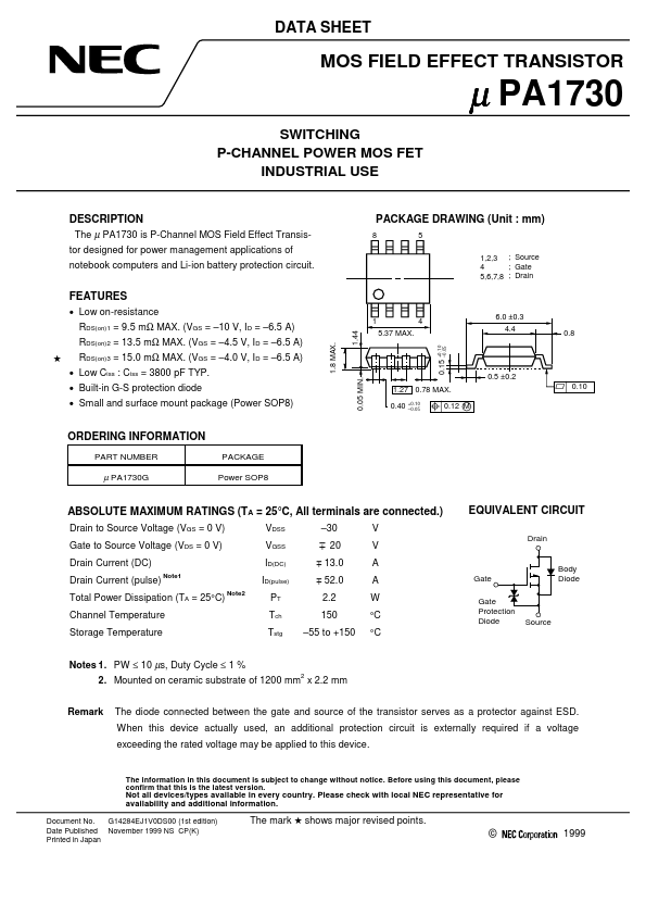
PACKAGE DRAWING (Unit : mm) 8 5 1,2,3 ; Source ; Gate 4 5,6,7,8 ; Drain FEATURES • Low on-resistance 1.44 RDS(on)1 = 9.5 mΩ MAX. (VGS = –10 V, ID = –6.5 A) 1.8 MAX. 1 5.37 MAX. 4 6.0 ±0.3 4.4 +0.10 –0.05 RDS(on)2 = 13.5 mΩ MAX. (VGS = –4.5 V, ID = –6.5 A) 5 RDS(on)3 = 15.0 mΩ MAX. (VGS = –4.0 V, ID = –6.5 A) • Low Ciss : Ciss = 3800 pF TYP. • Built-in G-S protection diode • Small and surface mount package (Power SOP8) 0.8 0.15 0.05 MIN. 0.5 ±0.2 0.10 1.27 0.78 MAX. 0.40 +0.10 –0.05 0.
Published: |