UPA2711GR
Description
The µ PA2711GR is P-Channel MOS Field Effect Transistor designed for power management applications of notebook computers and Li-ion battery protection circuit.
Key Features
- Low on-state resistance RDS(on)1 = 9 mΩ MAX. (VGS = -10 V, ID = -6.5 A) RDS(on)2 = 15 mΩ MAX. (VGS = -4.5 V, ID = -6.5 A) RDS(on)3 = 20 mΩ MAX. (VGS = -4.0 V, ID = -6.5 A)
- Low Ciss: Ciss = 2450 pF TYP.
- Small and surface mount package (Power SOP8)
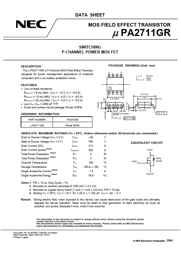
- 0 ±0.3 4.4 +0.10 -0.05 1 4 5.37 MAX.
- 8 MAX.
- 05 MIN.
- 5 ±0.2 0.10