P2504EDG Overview
Key Features
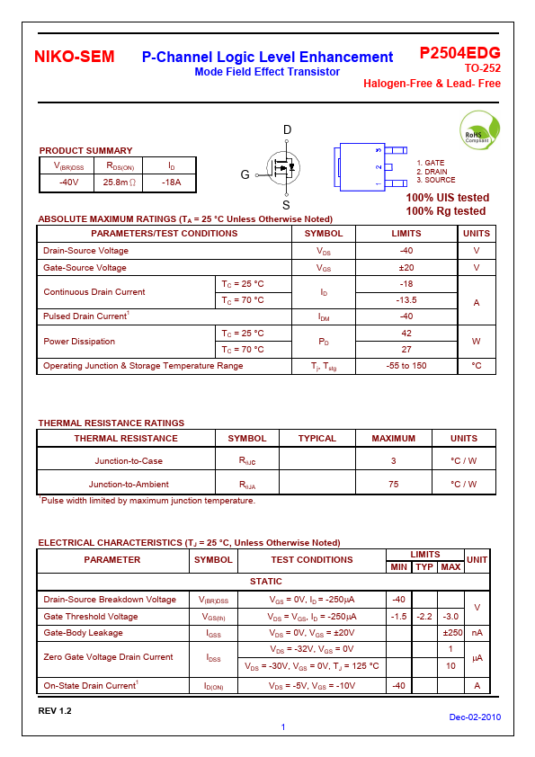
- 40 -1.5 -2.2
| Part | P2504EDG |
|---|---|
| Description | P-Channel Logic FET |
| Manufacturer | NIKO-SEM |
| Size | 711.56 KB |
| Seller | Inventory | Price Breaks | Buy |
|---|---|---|---|
| UnikeyIC | 400000 | 50+ : 0.2611 USD 100+ : 0.2568 USD 150+ : 0.2503 USD |
View Offer |
| Unikeyic (ICkey) | 400000 | 50+ : 0.2611 USD 100+ : 0.2568 USD 150+ : 0.2503 USD |
View Offer |
| Part Number | Manufacturer | Description |
|---|---|---|
| P2504EDG | UNIKC | P-Channel MOSFET |
| P2504EI | UNIKC | MOSFET |
| P2504BDG | UNIKC | N-Channel MOSFET |
| P2500M | Taiwan Semiconductor | Glass Passivated Rectifier |
| P2500SCLRP | Littelfuse | SIDACtor Protection Thyristors |