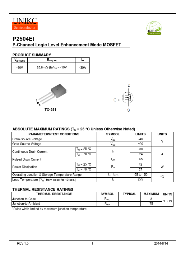
P2504EI Overview
Key Features
- 55 to 150 275
| Part | P2504EI |
|---|---|
| Description | MOSFET |
| Category | MOSFET |
| Manufacturer | UNIKC |
| Size | 475.84 KB |
| Seller | Inventory | Price Breaks | Buy |
|---|---|---|---|
| UnikeyIC | 400000 | 100+ : 0.2393 USD 200+ : 0.2353 USD 300+ : 0.2293 USD |
View Offer |
| Unikeyic (ICkey) | 400000 | 100+ : 0.2393 USD 200+ : 0.2353 USD 300+ : 0.2293 USD |
View Offer |
| Part Number | Manufacturer | Description |
|---|---|---|
| P2504EDG | NIKO-SEM | P-Channel Logic FET |
| P2504BDG | NIKO-SEM | N-Channel Logic FET |
| P2500M | Taiwan Semiconductor | Glass Passivated Rectifier |
| P2500SCLRP | Littelfuse | SIDACtor Protection Thyristors |
| P2503NPG | NIKO-SEM | N- & P-Channel Field Effect Transistor |