P2806BD
NIKO-SEM
N-Channel Enhancement Mode Field Effect Transistor
TO-252
Halogen-Free & Lead-Free
PRODUCT SUMMARY
V(BR)DSS
RDS(ON)
60V 28mΩ
ID 30A
ABSOLUTE MAXIMUM RATINGS (TA = 25 °C Unless Otherwise Noted)
PARAMETERS/TEST CONDITIONS
SYMBOL
Gate-Source Voltage
Continuous Drain Current Pulsed Drain Current1
TC = 25 °C TC = 100 °C
Avalanche Current
Avalanche Energy
L = 0.1m H
Power Dissipation
TC = 25 °C TC = 100 °C
Operating Junction & Storage Temperature Range
IDM IAS EAS
Tj, Tstg
THERMAL RESISTANCE RATINGS THERMAL RESISTANCE
SYMBOL
Junction-to-Case
RθJC
Junction-to-Ambient
RθJA
1Pulse width limited by maximum junction temperature.
TYPICAL
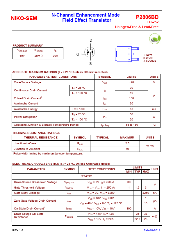
1. GATE 2. DRAIN 3. SOURCE
LIMITS ±20 30 19 100 30 43 50 20
-55 to 150
UNITS V
A m J W...