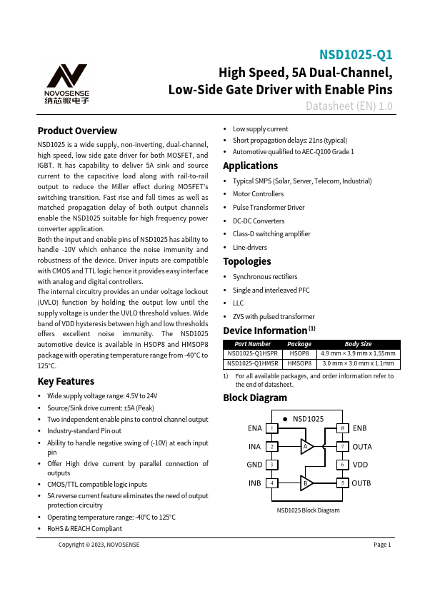
Datasheet4U Logo Datasheet4U.com

NSD1025-Q1 - Low-Side Gate Driver

General Description

9 6.1 OVERVIEW 9 6.2 FUNCTIONAL BLOCK DIAGRAM10 6.3 FEATURE DESCRIPTION10 6.3.1 Supply Voltage

Key Features

  • Wide supply voltage range: 4.5V to 24V.
  • Source/Sink drive current: ±5A (Peak).
  • Two independent enable pins to control channel output.
  • Industry-standard Pin out.
  • Ability to handle negative swing of (-10V) at each input pin.
  • Offer High drive current by parallel connection of outputs.
  • CMOS/TTL compatible logic inputs.
  • 5A reverse current feature eliminates the need of output protection circuitry.
  • Operating temperature range: -40°C to 125°C.
  • RoHS & R.

📥 Download Datasheet

Full PDF Text Transcription (Reference)

The following content is an automatically extracted verbatim text from the original manufacturer datasheet and is provided for reference purposes only.

View original datasheet text
NSD1025-Q1 High Speed, 5A Dual-Channel, Low-Side Gate Driver with Enable Pins Datasheet (EN) 1.0 Product Overview NSD1025 is a wide supply, non-inverting, dual-channel, high speed, low side gate driver for both MOSFET, and IGBT. It has capability to deliver 5A sink and source current to the capacitive load along with rail-to-rail output to reduce the Miller effect during MOSFET’s switching transition. Fast rise and fall times as well as matched propagation delay of both output channels enable the NSD1025 suitable for high frequency power converter application. Both the input and enable pins of NSD1025 has ability to handle -10V which enhance the noise immunity and robustness of the device.