NXP Semiconductors 74ALVT16823
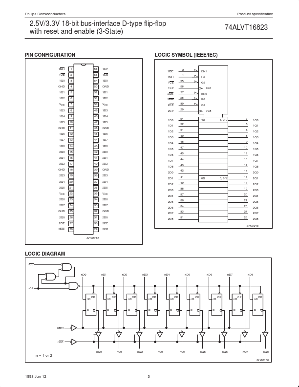
The 74ALVT16823 18-bit bus interface register is designed to eliminate the extra packages required to buffer existing registers and provide extra data width for wider data/address paths of buses carrying parity. The 74ALVT16823 has two 9-bit wide buffered registers with Clock Enable (nCE) and Master Reset (nMR) which are ideal for parity bus interfacing in high microprogrammed systems. The registers are fully edge-triggered.| Part No. | 74ALVT16823 |
|---|---|
| Datasheet | 74ALVT16823 Download |
| Manufacturer |  NXP Semiconductors |
| Description | 18-bit bus-interface D-type flip-flop |
| Buy | Stock & Price |
FEATURES
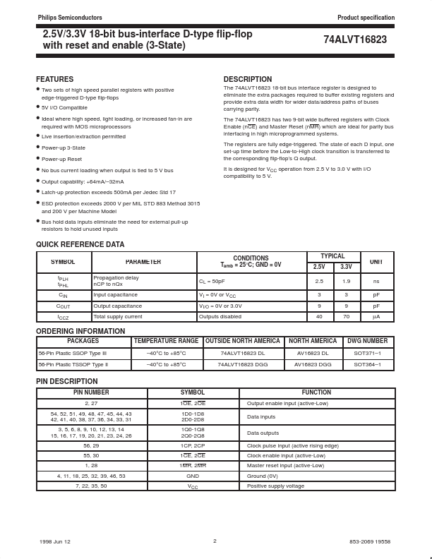
● Two sets of high speed parallel registers with positive edge-triggered D-type flip-flopsDESCRIPTION
The registers are fully edge-triggered. The state of each D input, one set-up time before the Low-to-High clock transition is transferred to the corresponding flip-flop’s Q output. It is designed for VCC operation from 2.5 V to 3.0 V with I/O compatibility to 5 V.● 5V I/O Compatible
● Ideal where high speed, light loading, or increased fan-in are required with MOS microprocessors
● Live insertion/extraction permitted
● Power-up 3-State
● Power-up Reset
● No bus current loading when output is tied to 5 V bus
● Output capability: +64mA/–32mA
● Latch-up protection exceeds 500mA per Jedec Std 17
● ESD protection exceeds 2000 V per MIL STD 883 Method 3015 and 200 V per Machine Model
● Bus hold data inputs eliminate the need for external pull-up resistors to hold unused inputs QUICK REFERENCE DATA SYMBOL tPLH tPHL CIN COUT ICCZ PARAMETER Propagation delay nCP to nQx Input capacita...