DESCRIPTION
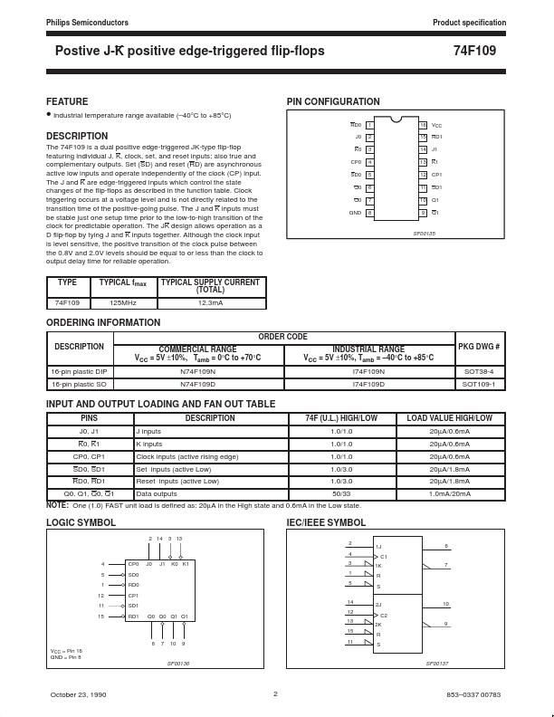
Set (SD) and reset (RD) are asynchronous active low inputs and operate independently of the clock (CP) input. Clock triggering occurs at a voltage level and is not directly related to the transition time of the positive-going pulse. The JK design allows operation as a D flip-flop by tying J and K inputs together. Although the clock input is level sensitive, the positive transition of the clock pulse between the 0.8V and 2.0V levels should be equal to or less than the clock to output delay time for reliable operation. TYPE 74F109 TYPICAL fmax 125MHz TYPICAL SUPPLY CURRENT (TOTAL) 12.3mA PIN CONFIGURATION RD0 J0 K0 CP0 SD0 Q0 Q0 GND 1 2 3 4 5 6 7 8 16 15 14 13 12 11 10 9 VCC RD1 J1 K1 CP1 SD1 Q1 Q1 SF00135 ORDERING INFORMATION ORDER CODE DESCRIPTION
16-pin plastic DIP 16-pin plastic SO COMMERCIAL RANGE VCC = 5V ±10%, Tamb = 0°C to +70°C N74F109N N74F109D INDUSTRIAL RANGE VCC = 5V ±10%, Tamb = –40°C to +85°C I74F109N I74F109D PKG DWG # SOT38-4 SOT109-1 INPUT AND OUTPUT LOADING... NXP Semiconductors