NXP Semiconductors 74F166
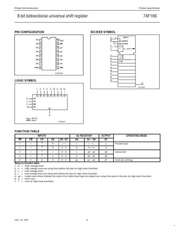
The 74F166 is a high speed 8–bit shift register that has fully synchronous serial parallel data entry selected by an active low parallel enable (PE) input. When the PE is low one setup time before the low–to–high clock transition, parallel data is entered into the register. When PE is high, data is entered into internal bit position Q0 from serial data input (Ds), and the remaining bits are shifted one place to the right (Q0 → Q1 → Q2, etc.) with each positive going clock transition.| Part No. | 74F166 |
|---|---|
| Datasheet | 74F166 Download |
| Manufacturer |  NXP Semiconductors |
| Description | 8-bit bidirectional universal shift register |
| Buy | Stock & Price |
FEATURES
● High impedance NPN base inputs for reduced loading●
●
●
●
●
● (20µA in high and low states) Synchronous parallel to serial applications Synchronous serial data input for easy expansion Clock enable for ”do nothing” mode Asynchronous master reset Expandable to 16 bits in 8–bit increments Industrial temperature range available (–40°C to +85°C)
DESCRIPTION
For expansion of the register in parallel to serial converters, the Q7 output is connected to the Ds input of the succeeding stage. The clock input is gated OR structure which allows one input to be used as an active–low clock enable (CE) input. The pin assignment for the CP and CE inputs is arbitrary and can be reversed for layout convenience. The low–to–high transition of CE input should only take place while the CP is high for predictable operation. A low on the master reset (MR) input overrides all other inputs and clears the register asynchronously, forcing all bit positions to a low state. TYPE 74F166 TYPICAL fmax 175M...