BLF2045
FEATURES
- High power gain
- Easy power control
- Excellent ruggedness
- Source on underside eliminates DC isolators, reducing mon mode inductance
- Designed for broadband operation. APPLICATIONS
- munication transmitter applications (PCN/PCS) in the 1.8 to 2.2 GHz frequency range.
PINNING
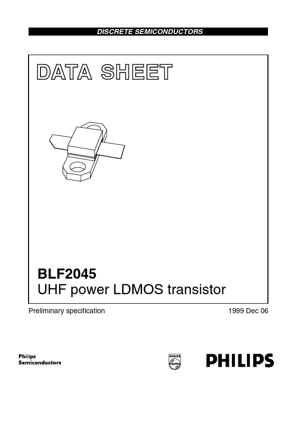
- SOT467C PIN 1 2 3 drain gate source, connected to flange DESCRIPTION
DESCRIPTION
Silicon N-channel enhancement mode lateral D-MOS transistor encapsulated in a 2-lead flange package (SOT467C) with a ceramic cap. The mon source is connected to the mounting flange.
2 Top view
MBK584
Fig.1 Simplified outline.
QUICK REFERENCE DATA RF performance at Th = 25 °C in a mon source test circuit. MODE OF OPERATION 2-tone, class-AB f (MHz) f1 = 2000; f2 = 2000.1 VDS (V) 26 PL (W) 30 (PEP) Gp (d B) >10 ηD (%) >30 dim (d Bc) ≤- 25
LIMITING VALUES In accordance with the Absolute Maximum Rating System (IEC 134). SYMBOL VDS VGS ID Tstg Tj PARAMETER drain-source voltage gate-source voltage drain...