NXP Semiconductors GTL2006
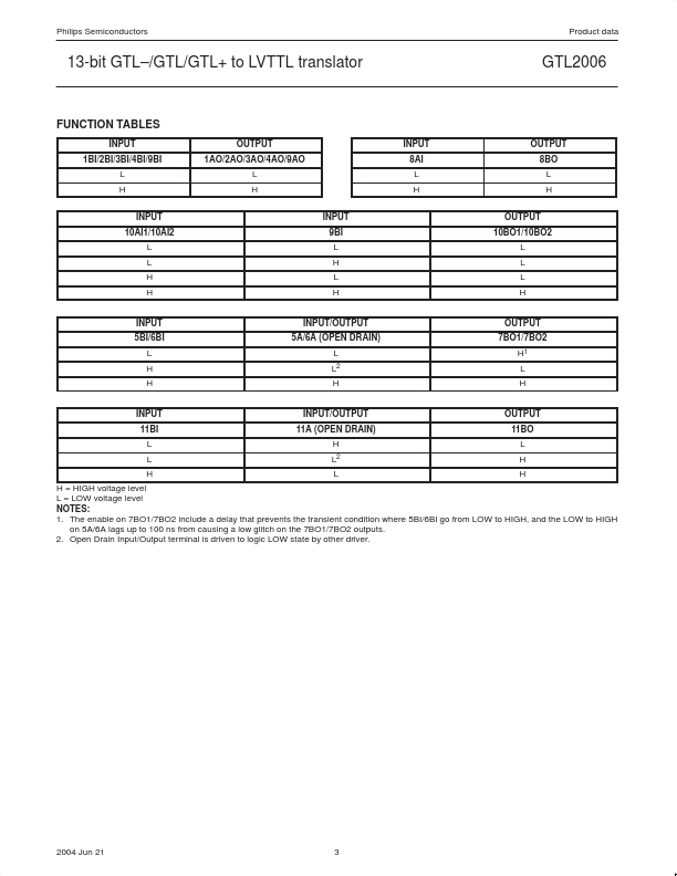
The GTL2006 is a 13-bit translator to interface between the 3.3 V LVTTL chip set I/O and the Xeon™ processor GTL–/GTL/GTL+ I/O. The GTL2006 is designed for platform health management in dual processor applications. The enable on 7BO1/7BO2 include a delay that prevents the transient condition where 5BI/6BI go from LOW to HIGH, and the LOW to HIGH on 5A/6A lags up to 100 ns from causing a low glitch on the 7BO1/7BO2 outputs.| Part No. | GTL2006 |
|---|---|
| Datasheet | GTL2006 Download |
| Manufacturer |  NXP Semiconductors |
| Description | 13-bit GTL-/GTL/GTL+ to LVTTL translator |
| Buy | Stock & Price |
FEATURES
● Operates as a GTL–/GTL/GTL+ to LVTTL sampling receiver or● 3.0 V to 3.6 V operation
● LVTTL I/O not 5 V tolerant
● Series termination on the LVTTL outputs of 30 Ω
● ESD protection exceeds 2000 V HBM per JESD22-A114, 200 V MM per JESD22-A115 and 250 V CDM per JESD22-C101 LVTTL to GTL–/GTL/GTL+ driver PIN CONFIGURATION VREF 1 1AO 2 2AO 3 5A 4 6A 5 8AI 6 11BI 7 11A 8 9BI 9 3AO 10 4AO 11 10AI1 12 10AI2 13 GND 14 28 27 26 25 24 23 22 21 20 19 18 17 16 15 VCC 1BI 2BI 7BO1 7BO2 8BO 11BO 5BI 6BI 3BI 4BI 10BOI 10BO2 9AO
● Latch-up testing is done to JESDEC Standard JESD78 which exceeds 500 mA
● Package offered: TSSOP28
DESCRIPTION
SW01091 Figure 1. Pin configuration PINDESCRIPTION
PIN NUMBER 1 2–6, 8, 10–13, 15 7, 9, 16, 17–27 14 28 SYMBOL VREF nAn nBn GND VCC NAME AND FUNCTION GTL reference voltage Data inputs/outputs (LVTTL) Data inputs/outputs (GTL–/GTL/GTL+) Ground (0 V) Positive supply voltage QUICK REFERENCE DATA SYMBOL tPLH tPHL CI/O PARAMETER Propagation delay An to Bn or B...