Datasheet Summary
DISCRETE SEMICONDUCTORS
DATA SHEET
M3D744
PBSS2515VS 15 V low VCEsat NPN double transistor
Product specification Supersedes data of 2001 Sep 13 2001 Nov 07
Philips Semiconductors
Product specification
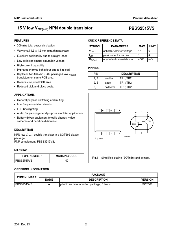
15 V low VCEsat NPN double transistor
Features
- 300 mW total power dissipation
- Very small 1.6 x 1.2 mm ultra thin package
- Excellent coplanarity due to straight leads
- Low collector-emitter saturation voltage
- High current capability
- Improved thermal behaviour due to flat lead
- Replaces two SC-75/SC-89 packaged low VCEsat transistors on same PCB area
- Reduces required PCB area
- Reduced pick and place costs. APPLICATIONS
- General purpose switching and muting
- Low frequency...