PHT6N03LT
PHT6N03LT is TrenchMOS transistor Logic level FET manufactured by NXP Semiconductors.
Philips Semiconductors
Product specification
Trench MOS™ transistor Logic level FET
Features
- ’Trench’ technology
- Very low on-state resistance
- Fast switching
- Stable off-state characteristics
- High thermal cycling performance
- Surface mounting package
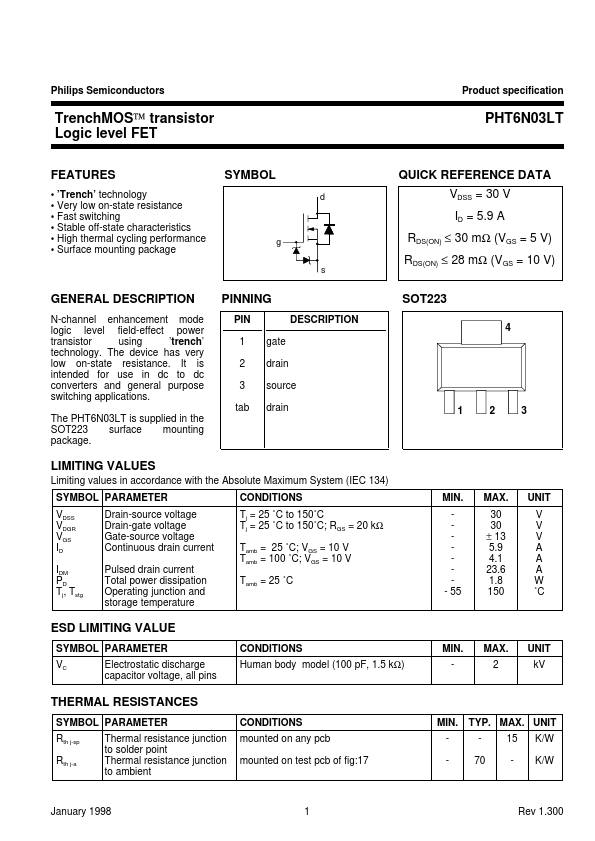
SYMBOL d
QUICK REFERENCE DATA VDSS = 30 V ID = 5.9 A g s
RDS(ON) ≤ 30 mΩ (VGS = 5 V) RDS(ON) ≤ 28 mΩ (VGS = 10 V) SOT223
DESCRIPTION
GENERAL DESCRIPTION
N-channel enhancement mode logic level field-effect power transistor using ’trench’ technology. The device has very low on-state resistance. It is intended for use in dc to dc converters and general purpose switching applications. The PHT6N03LT is supplied in the SOT223 surface mounting package.
PINNING
PIN 1 2 3 tab gate drain source drain
LIMITING VALUES
Limiting values in accordance with the Absolute Maximum System (IEC 134) SYMBOL PARAMETER VDSS VDGR VGS ID IDM PD Tj, Tstg Drain-source voltage Drain-gate voltage Gate-source voltage Continuous drain current Pulsed drain current Total power dissipation Operating junction and storage temperature CONDITIONS Tj = 25 ˚C to 150˚C Tj = 25 ˚C to 150˚C; RGS = 20 kΩ Tamb = 25 ˚C; VGS = 10 V Tamb = 100 ˚C; VGS = 10 V Tamb = 25 ˚C MIN.
- 55 MAX. 30 30 ± 13 5.9 4.1 23.6 1.8 150 UNIT V V V A A A W ˚C
ESD LIMITING VALUE
SYMBOL PARAMETER VC Electrostatic discharge capacitor voltage, all pins CONDITIONS Human body model (100 p F, 1.5 kΩ) MIN. MAX. 2 UNIT k V
THERMAL RESISTANCES
SYMBOL PARAMETER Rth j-sp Rth j-a Thermal resistance junction to solder point Thermal resistance junction to ambient CONDITIONS mounted on any pcb mounted on test pcb of fig:17 MIN. TYP. MAX. UNIT 70 15 K/W K/W
January 1998
Rev 1.300
Philips Semiconductors
Product specification
Trench MOS™ transistor Logic level...