PHT6N06LT
PHT6N06LT is TrenchMOS transistor Logic level FET manufactured by NXP Semiconductors.
Philips Semiconductors
Product specification
Trench MOS™ transistor Logic level FET
GENERAL DESCRIPTION
N-channel enhancement mode logic level field-effect power transistor in a plastic envelope suitable for surface mounting. The device Features very low on-state resistance and has integral zener diodes giving ESD protection. It is intended for use in DC-DC converters and general purpose switching applications.
QUICK REFERENCE DATA
SYMBOL VDS ID Ptot Tj RDS(ON) PARAMETER Drain-source voltage Drain current (DC) Tsp = 25 ˚C Drain current (DC) Tamb = 25 ˚C Total power dissipation Junction temperature Drain-source on-state resistance VGS = 5 V MAX. 55 5.5 2.5 8.3 150 150 UNIT V A A W ˚C mΩ
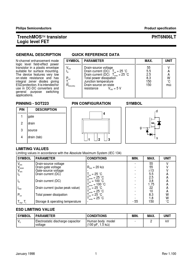
PINNING
- SOT223
PIN 1 2 3 4 gate drain source drain (tab) DESCRIPTION
PIN CONFIGURATION
SYMBOL d g s
LIMITING VALUES
Limiting values in accordance with the Absolute Maximum System (IEC 134) SYMBOL VDS VDGR VGS ID ID IDM Ptot Tstg, Tj PARAMETER Drain-source voltage Drain-gate voltage Gate-source voltage Drain current (DC) Drain current (DC) Drain current (pulse peak value) Total power dissipation Storage & operating temperature CONDITIONS RGS = 20 kΩ Tsp = 25 ˚C Tamb = 25 ˚C Tsp = 100 ˚C Tamb = 100 ˚C Tsp = 25 ˚C Tamb = 25 ˚C Tsp = 25 ˚C Tamb = 25 ˚C MIN.
- 55 MAX. 55 55 ±13 5.5 2.5 3.8 1.75 22 10 8.3 1.8 150 UNIT V V V A A A A A A W W ˚C
ESD LIMITING VALUE
SYMBOL VC PARAMETER Electrostatic discharge capacitor voltage CONDITIONS Human body model (100 p F, 1.5 kΩ) MIN. MAX. 2 UNIT k V
January 1998
Rev 1.100
Philips Semiconductors
Product specification
Trench MOS™ transistor Logic level FET
THERMAL RESISTANCES
SYMBOL Rth j-sp Rth j-amb PARAMETER From junction to solder point From junction to ambient CONDITIONS Mounted on any PCB Mounted on PCB of Fig.17 TYP. 12
- PHT6N06LT
MAX. 15 70
UNIT K/W K/W
STATIC CHARACTERISTICS
Tj= 25˚C unless otherwise specified SYMBOL V(BR)DSS VGS(TO) IDSS IGSS ±V(BR)GSS RDS(ON) PARAMETER Drain-source breakdown voltage...