PHT6NQ10T
PHT6NQ10T is N-channel TrenchMOS transistor manufactured by NXP Semiconductors.
Philips Semiconductors
Product specification
N-channel Trench MOS™ transistor
Features
- ’Trench’ technology
- Low on-state resistance
- Fast switching
- Low thermal resistance
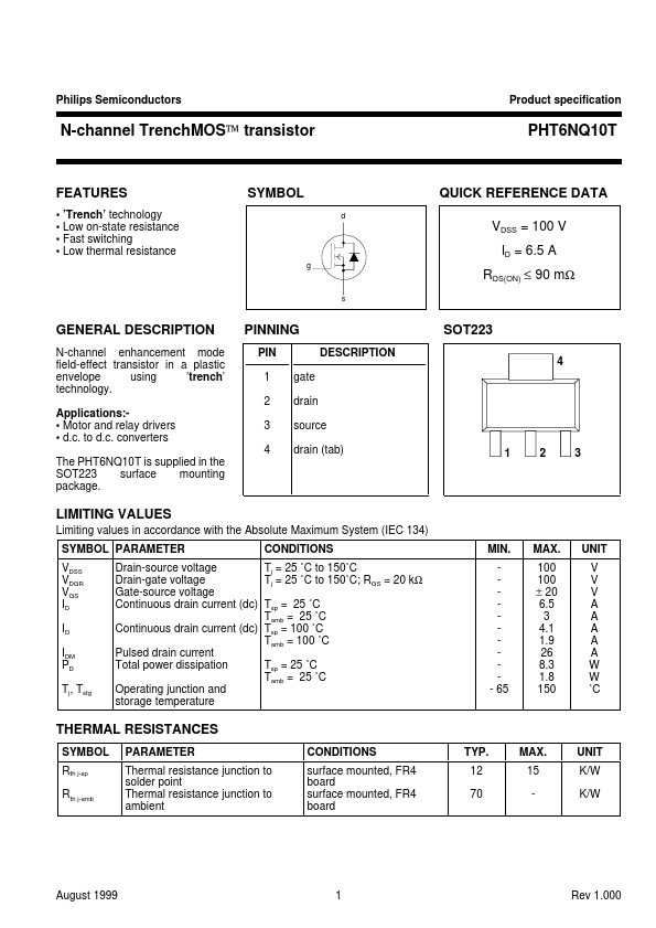
SYMBOL d
QUICK REFERENCE DATA VDSS = 100 V ID = 6.5 A g
RDS(ON) ≤ 90 mΩ s
GENERAL DESCRIPTION
N-channel enhancement mode field-effect transistor in a plastic envelope using ’trench’ technology. Applications:- Motor and relay drivers
- d.c. to d.c. converters The PHT6NQ10T is supplied in the SOT223 surface mounting package.
PINNING
PIN 1 2 3 4 gate drain source drain (tab) DESCRIPTION
SOT223
LIMITING VALUES
Limiting values in accordance with the Absolute Maximum System (IEC 134) SYMBOL PARAMETER VDSS VDGR VGS ID ID IDM PD Tj, Tstg CONDITIONS MIN.
- 65 MAX. 100 100 ± 20 6.5 3 4.1 1.9 26 8.3 1.8 150 UNIT V V V A A A A A W W ˚C Drain-source voltage Tj = 25 ˚C to 150˚C Drain-gate voltage Tj = 25 ˚C to 150˚C; RGS = 20 kΩ Gate-source voltage Continuous drain current (dc) Tsp = 25 ˚C Tamb = 25 ˚C Continuous drain current (dc) Tsp = 100 ˚C Tamb = 100 ˚C Pulsed drain current Total power dissipation Tsp = 25 ˚C Tamb = 25 ˚C Operating junction and storage temperature
THERMAL RESISTANCES
SYMBOL Rth j-sp Rth j-amb PARAMETER Thermal resistance junction to solder point Thermal resistance junction to ambient CONDITIONS surface mounted, FR4 board surface mounted, FR4 board TYP. 12 70 MAX. 15 UNIT K/W K/W
August 1999
Rev 1.000
Philips Semiconductors
Product specification
N-channel Trench MOS™ transistor
ELECTRICAL CHARACTERISTICS
Tj= 25˚C unless otherwise specified SYMBOL PARAMETER V(BR)DSS VGS(TO) RDS(ON) IGSS IDSS Qg(tot) Qgs Qgd td on tr td off tf Ld Ls Ciss Coss Crss Drain-source breakdown voltage Gate threshold voltage CONDITIONS VGS = 0 V; ID = 0.25 m A; Tj = -55˚C VDS = VGS; ID = 1 m A Tj = 150˚C Tj = -55˚C Drain-source on-state VGS = 10 V; ID = 3 A resistance Gate source leakage current VGS = ±10 V; VDS = 0 V Zero gate voltage drain VDS = 100 V; VGS = 0...