N04L163WC1A
N04L163WC1A is 4Mb Ultra-Low Power Asynchronous CMOS SRAM manufactured by NanoAmp Solutions.
Overview
The N04L163WC1A is an integrated memory device containing a 4 Mbit Static Random Access Memory organized as 262,144 words by 16 bits. The device is designed and fabricated using Nano Amp’s advanced CMOS technology to provide both high-speed performance and ultra-low power. The device operates with a single chip enable (CE) control and output enable (OE) to allow for easy memory expansion. Byte controls (UB and LB) allow the upper and lower bytes to be accessed independently. The N04L163WC1A is optimal for various applications where low-power is critical such as battery backup and hand-held devices. The device can operate over a very wide temperature range of -40o C to +85o C and is available in JEDEC standard packages patible with other standard 256Kb x 16 SRAMs.
Features
- Single Wide Power Supply Range 2.3 to 3.6 Volts
- Very low standby current 4.0µA at 3.0V (Typical)
- Very low operating current 2.0m A at 3.0V and 1µs (Typical)
- Very low Page Mode operating current 0.8m A at 3.0V and 1µs (Typical)
- Simple memory control Single Chip Enable (CE) Byte control for independent byte operation Output Enable (OE) for memory expansion
- Low voltage data retention Vcc = 1.8V
- Very fast output enable access time 25ns OE access time
- Automatic power down to standby mode
- TTL patible three-state output driver
- pact space saving BGA package available
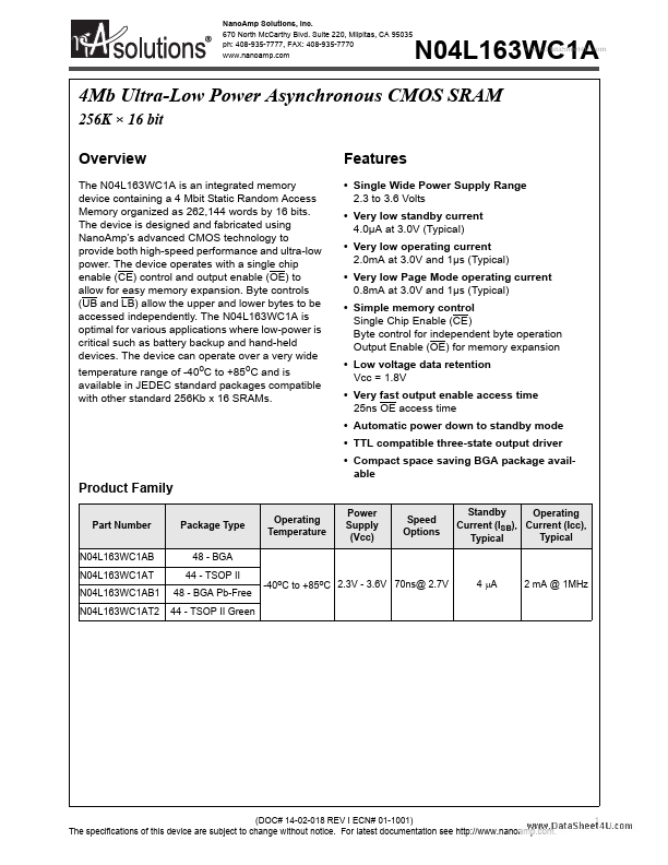
Product Family
Part Number N04L163WC1AB N04L163WC1AT N04L163WC1AB1 N04L163WC1AT2 Package Type 48
- BGA 44
- TSOP II 48
- BGA Pb-Free 44
- TSOP II Green -40o C to +85o C 2.3V
- 3.6V 70ns@ 2.7V 4 µA 2 m A @ 1MHz Operating Temperature Power Supply (Vcc) Speed Options Standby Operating Current (ISB), Current (Icc), Typical Typical
(DOC# 14-02-018 REV I ECN# 01-1001) The specifications of this device are subject to change without notice. For latest documentation see http://.nanoamp..
Nano Amp Solutions, Inc. Pin Configurations
A4 A3 A2 A1 A0 CE I/O0 I/O1 I/O2 I/O3 VCC VSS I/O4 I/O5 I/O6 I/O7 WE A16 A15 A14 A13 A12 1 2 3...