N04Q16YYC2B
N04Q16YYC2B is 4Mb Ultra-Low Power Asynchronous CMOS SRAM manufactured by NanoAmp Solutions.
Overview
The N04Q16yy C2B are ultra-low power memory devices containing a 4 Mbit Static Random Access Memory organized as 262,144 words by 16 bits. The device is designed and fabricated using Nano Amp’s advanced CMOS technology to provide ultra-low active and standby power. The device operates with two chip enable (CE1 and CE2) controls and output enable (OE) to allow for easy memory expansion. Byte controls (UB and LB) allow the upper and lower bytes to be accessed independently. The 4Mb SRAM is optimized for the ultimate in low power and is suited for various applications where ultra-lowpower is critical such as medical applications, battery backup and power sensitive hand-held devices. The unique page mode operation saves active operating power and the dual power supply rails allow very low voltage operation while maintaining 3V I/O capability. The device can operate over a very wide temperature range of 0o C to +70o C for the lowest power and is also available in the industrial range of -40o C to +85o C. The devices are available in standard BGA and TSOP packages. The devices are also available as Known Good Die (KGD) for embedded package applications.
Features
- Multiple Power Supply Ranges 1.1V
- 1.3V 1.65V
- 1.95V 2.3V
- 2.7V 2.7V
- 3.6V
- Dual Vcc / Vcc Q Power Supplies 1.2V Vcc with 3V Vcc Q 1.8V Vcc with 3V Vcc Q 2.5V Vcc with 3V Vcc Q
- Very low standby current 50n A typical for 1.2V operation
- Very low operating current 400µA typical for 1.2V operation at 1µs
- Very low Page Mode operating current 80µA typical for 1.2V operation at 1µs
- Simple memory control Dual Chip Enables (CE1 and CE2) Byte control for independent byte operation Output Enable (OE) for memory expansion
- Automatic power down to standby mode
- BGA, TSOP and KGD options
- Ro HS pliant
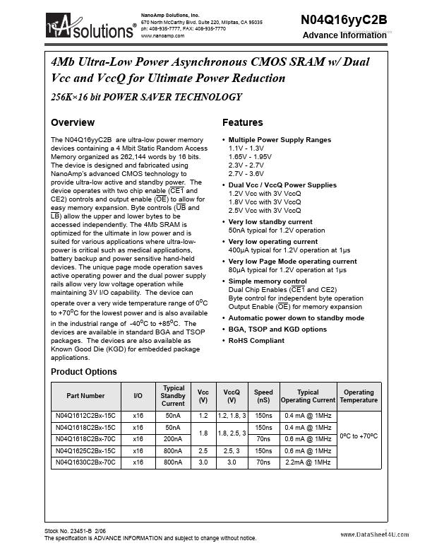
Product Options
Part Number N04Q1612C2Bx-15C N04Q1618C2Bx-15C N04Q1618C2Bx-70C N04Q1625C2Bx-15C N04Q1630C2Bx-70C I/O x16 x16 x16 x16 x16 Typical Standby Current 50n A 50n A 200n A 800n A 800n A Vcc (V) 1.2 1.8 2.5 3.0...