CD4514BM
Description
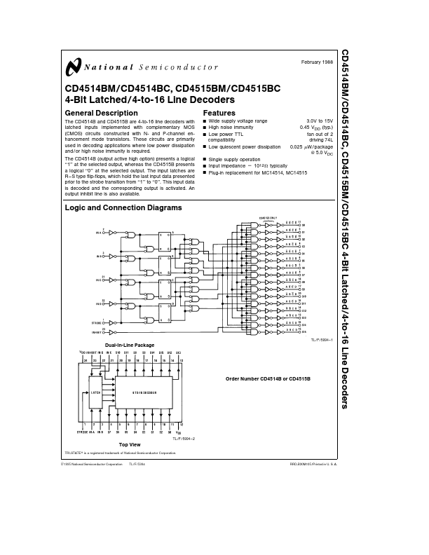
The CD4514B and CD4515B are 4-to-16 line decoders with latched inputs implemented with complementary MOS (CMOS) circuits constructed with N- and P-channel enhancement mode transistors These circuits are primarily used in decoding applications where low power dissipation and or high noise immunity is required The CD4514B (output active high option) presents a logical ‘‘1’’ at the selected output whereas the CD4515B presents a logical ‘‘0’’ at the selected output The input latches are R - S type flip-flops which hold the last input data presented prior to the strobe transition from ‘‘1’’ to ‘‘0’’ This input data is decoded and the corresponding output is activated An output inhibit line is also available.