DS90LV110AT Overview
Description
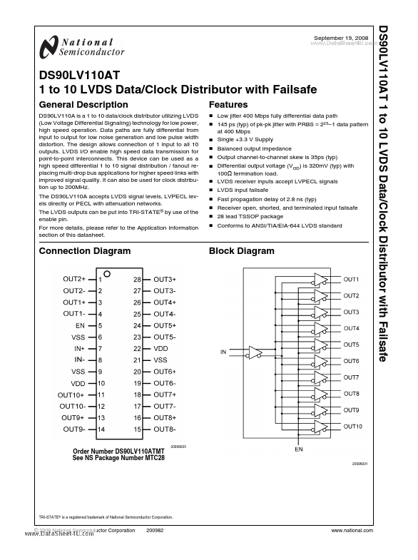
DS90LV110A is a 1 to 10 data/clock distributor utilizing LVDS (Low Voltage Differential Signaling) technology for low power, high speed operation. Data paths are fully differential from input to output for low noise generation and low pulse width distortion.
Key Features
- Low jitter 400 Mbps fully differential data path
- 145 ps (typ) of pk-pk jitter with PRBS = 223-1 data pattern