GENERAL DESCRIPTION
FEATURES
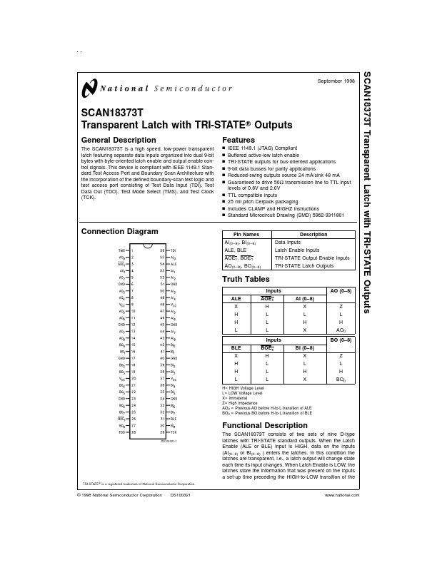
n n n n n n n n n n IEEE 1149.1 (JTAG) Compliant Buffered active-low latch enable TRI-STATE outputs for bus-oriented applications 9-bit data busses for parity applications Reduced-swing outputs source 24 mA/sink 48 mA Guaranteed to drive 50Ω transmission line to TTL input levels of 0.8V and 2.0V TTL compatible inputs 25 mil pitch Cerpack packaging Includes CLAMP and HIGHZ instructions Standard Microcircuit Drawing (SMD) 5962-9311801 Connection Diagram Pin Names AI(0–8), BI(0–8) ALE, BLE AOE1, BOE1 AO(0–8), BO(0–8) DESCRIPTION
Data Inputs Latch Enable Inputs TRI-STATE Output Enable Inputs TRI-STATE Latch Outputs Truth Tables Inputs ALE X H H L AOE1 H L L L Inputs BLE X H H L BOE1 H L L L BI (0–8) X L H X Z L H BO0 AI (0–8) X L H X Z L H AO0 BO (0–8) AO (0–8) H = HIGH Voltage Level L = LOW Voltage Level X = Immaterial Z = High Impedance AO0 = Previous AO before H-to-L transition of ALE BO0 = Previous BO before H-to-L transition of BLE Functional DESCRIPTION
DS100321-1 The SCAN18373T consists of two sets of nine D-type latches with TRI-STATE standard outputs. National Semiconductor