54ACT374
54ACT374 is Octal D Flip-Flop manufactured by National Semiconductor.
- Part of the 54AC374 comparator family.
- Part of the 54AC374 comparator family.
Description
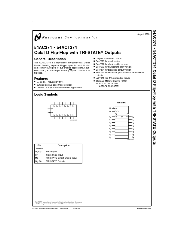
The ’AC/’ACT374 is a high-speed, low-power octal D-type flip-flop featuring separate D-type inputs for each flip-flop and TRI-STATE outputs for bus-oriented applications. A buffered Clock (CP) and Output Enable (OE) are mon to all flip-flops. Outputs source/sink 24 m A See ’273 for reset version See ’377 for clock enable version See ’373 for transparent latch version See ’574 for broadside pinout version See ’564 for broadside pinout version with inverted outputs n ’ACT374 has TTL-patible inputs n Standard Military Drawing (SMD)
- ’AC374: 5962-87694
- ’ACT374: 5962-87631 n n n n n n
Features n ICC and IOZ reduced by 50% n Buffered positive edge-triggered clock n TRI-STATE outputs for bus-oriented applications
Logic Symbols
IEEE/IEC
DS100289-1
DS100289-2
Pin Names D0- D7 CP OE O0- O7 Data Inputs
Description
Clock Pulse Input TRI-STATE Output Enable Input TRI-STATE Outputs
TRI-STATE ® is a registered trademark of National Semiconductor Corporation. FACT ® is a registered trademark of Fairchild Semiconductor Corporation.
© 1998 National Semiconductor Corporation
DS100289
.national.
Connection Diagrams
Pin Assignment for DIP and Flatpak Pin Assignment for LCC
DS100289-4 DS100289-3
Functional Description
The ’AC/’ACT374 consists of eight edge-triggered flip-flops with individual D-type inputs and TRI-STATE true outputs. The buffered clock and buffered Output Enable are mon to all flip-flops. The eight flip-flops will store the state of their individual D inputs that meet the setup and hold time requirements on the LOW-to-HIGH Clock (CP) transition. With the Output Enable (OE) LOW, the contents of the eight flip-flops are available at the outputs. When the OE is HIGH, the outputs go to the high impedance state. Operation of the OE input does not affect the state of the flip-flops.
Truth Table
Inputs Dn H L X CP
Outputs OE L L H On H L Z
H = HIGH Voltage Level L = LOW Voltage Level X = Immaterial Z = High Impedance N = LOW-to-HIGH...