Datasheet4U.com
🌙
2N3906 Datasheet | onsemi
Part:
2N3906
Description:
PNP General-Purpose Amplifier
Manufacturer:
onsemi
Size:
247.42 KB
2N3906 Datasheet (PDF) Download
onsemi
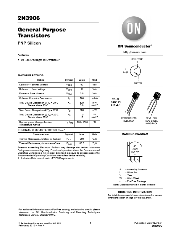
2N3906
Key Features
Pb-Free Packages are Available*
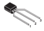
Representative 2N3906 image (package may vary by manufacturer)
Datasheets by Manufacturer
2N3906S
— Inchange Semiconductor — PNP Transistor
2N3906
— Kodenshi AUK Group — PNP Silicon Transistor
2N3906S
— KEC — EPITAXIAL PLANAR PNP TRANSISTOR
2N3906
— Fairchild Semiconductor — PNP Transistor
2N3906
— NTE Electronics — Silicon PNP Transistor
2N3906SC
— KEC — EPITAXIAL PLANAR PNP TRANSISTOR
2N3906
— Central Semiconductor — SILICON PNP TRANSISTORS
2N3906
— Micro Commercial Components — PNP Transistor
2N3906
— Motorola Semiconductor — Transistors
2N3906-G
— Comchip Technology — General Purpose transistor
×
Close