FDMS7620S
FDMS7620S is Dual N-Channel MOSFET manufactured by onsemi.
Features
Q1: N-Channel
- Max r DS(on) = 20.0 mΩ at VGS = 10 V, ID = 10.1 A
- Max r DS(on) = 30.0 mΩ at VGS = 4.5 V, ID = 7.5 A Q2: N-Channel
- Max r DS(on) = 11.2 mΩ at VGS = 10 V, ID = 12.4 A
- Max r DS(on) = 14.2 mΩ at VGS = 4.5 V, ID = 10.9 A
- Pinout optimized for simple PCB design
- Thermally efficient dual Power 56 Package
- Ro HS pliant
General Description
This device includes two specialized MOSFETs in a unique dual Power 56 package. It is designed to provide an optimal synchronous buck power stage in terms of efficiency and PCB utilization. The low switching loss “High Side” MOSFET is plementory by a low conduction loss “Low Side” Sync FET.
Applications
Synchronous Buck Converter for:
- Notebook System Power
- General Purpose Point of Load
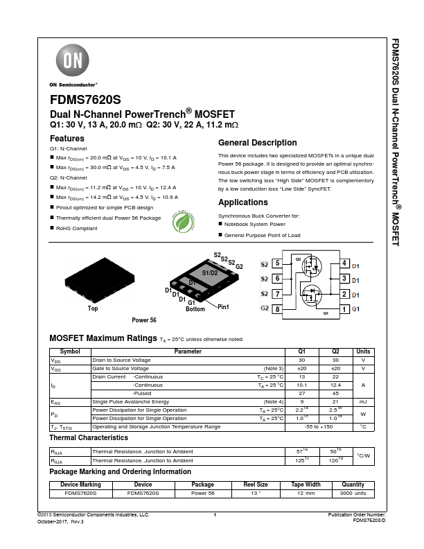
S2
S2 S2
Q2
G2
S1/D2
D1
D1 D1
D1 G1
Top
Bottom Pin1
Q1
Power 56
MOSFET Maximum Ratings TA = 25°C unless otherwise noted
Symbol VDS VGS
EAS PD TJ, TSTG
Parameter Drain to Source Voltage Gate to Source Voltage Drain Current...