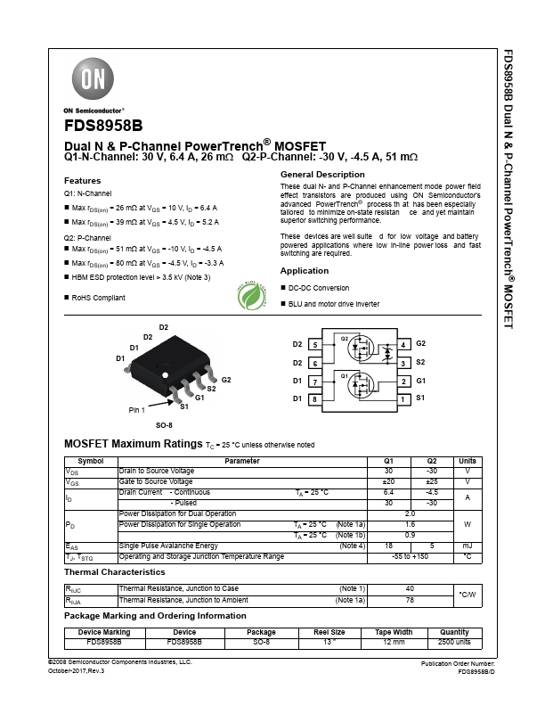
Datasheet4U Logo Datasheet4U.com

FDS8958B - Dual N & P-Channel Power MOSFET

Datasheet Summary

Description

These dual N- and P-Channel enhancement mode power field effect transistors are produced using ON Semiconductor's advanced PowerTrench® process th at has been especially tailored to minimize on-state resistan ce and yet maintain superior switching performance.

Features

  • Q1: N-Channel.
  • Max rDS(on) = 26 mΩ at VGS = 10 V, ID = 6.4 A.
  • Max rDS(on) = 39 mΩ at VGS = 4.5 V, ID = 5.2 A Q2: P-Channel.
  • Max rDS(on) = 51 mΩ at VGS = -10 V, ID = -4.5 A.
  • Max rDS(on) = 80 mΩ at VGS = -4.5 V, ID = -3.3 A.
  • HBM ESD protection level > 3.5 kV (Note 3).
  • RoHS Compliant General.

📥 Download Datasheet

Datasheet preview – FDS8958B

Datasheet Details

Part number FDS8958B
Manufacturer ON Semiconductor
File Size 698.92 KB
Description Dual N & P-Channel Power MOSFET
Datasheet download datasheet FDS8958B Datasheet
Additional preview pages of the FDS8958B datasheet.
Other Datasheets by ON Semiconductor

Full PDF Text Transcription

Click to expand full text
FDS8958B Dual N & P-Channel PowerTrench® MOSFET FDS8958B Dual N & P-Channel PowerTrench® MOSFET Q1-N-Channel: 30 V, 6.4 A, 26 mΩ Q2-P-Channel: -30 V, -4.5 A, 51 mΩ Features Q1: N-Channel „ Max rDS(on) = 26 mΩ at VGS = 10 V, ID = 6.4 A „ Max rDS(on) = 39 mΩ at VGS = 4.5 V, ID = 5.2 A Q2: P-Channel „ Max rDS(on) = 51 mΩ at VGS = -10 V, ID = -4.5 A „ Max rDS(on) = 80 mΩ at VGS = -4.5 V, ID = -3.3 A „ HBM ESD protection level > 3.5 kV (Note 3) „ RoHS Compliant General Description These dual N- and P-Channel enhancement mode power field effect transistors are produced using ON Semiconductor's advanced PowerTrench® process th at has been especially tailored to minimize on-state resistan ce and yet maintain superior switching performance.
Published: |