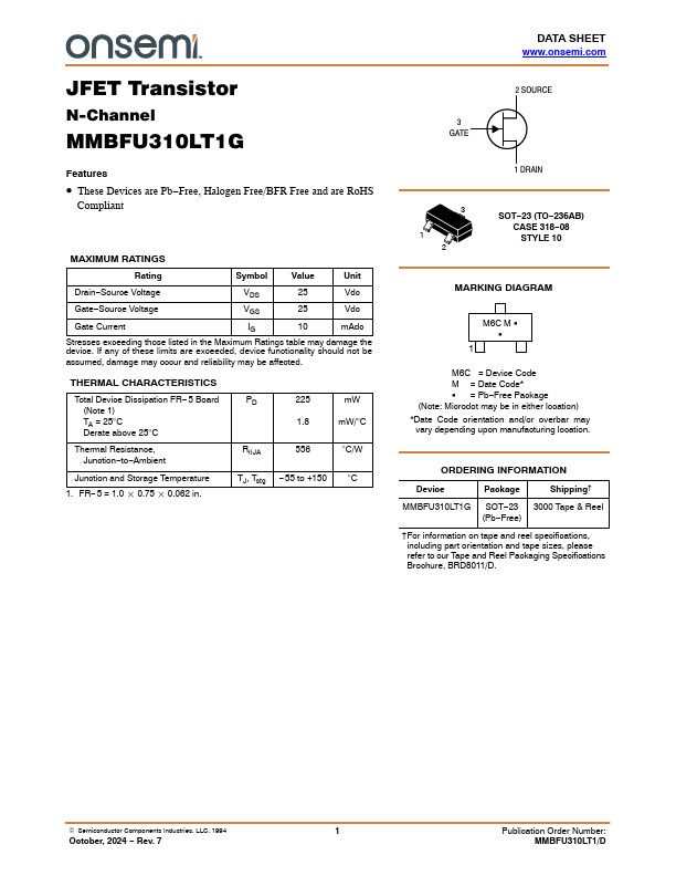
MMBFU310LT1G Overview
Key Features
- These Devices are Pb-Free, Halogen Free/BFR Free and are RoHS Compliant
| Part | MMBFU310LT1G |
|---|---|
| Description | N-Channel JFET Transistor |
| Category | Transistor |
| Manufacturer | onsemi |
| Size | 194.17 KB |
| Part Number | Manufacturer | Description |
|---|---|---|
| MMBFU310LT1 | onsemi | JFET Transistor |
| MMBFU310LT1 | Motorola Semiconductor | JFET Transistor |
| MMBFU310 | Motorola Semiconductor | FET TRANSISTOR |