MMBFU310LT1 Overview
Key Features
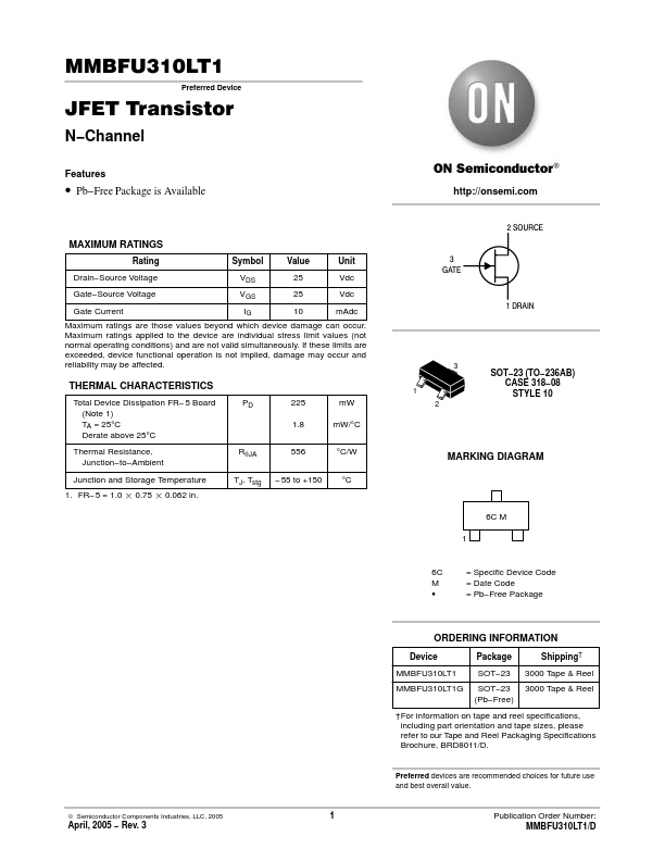
- Pb-Free Package is Available 2 SOURCE
| Part | MMBFU310LT1 |
|---|---|
| Description | JFET Transistor |
| Category | Transistor |
| Manufacturer | onsemi |
| Size | 119.70 KB |
| Part Number | Manufacturer | Description |
|---|---|---|
| MMBFU310LT1 | Motorola Semiconductor | JFET Transistor |
| MMBFU310 | Motorola Semiconductor | FET TRANSISTOR |