MPSH17 Overview
Key Specifications
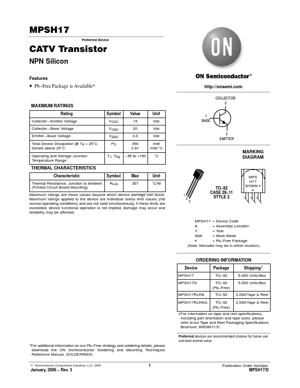
Package: TO-92-3
Max Operating Temp: 150 °C
Min Operating Temp: -55 °C
Key Features
- Pb-Free Package is Available*
| Part | MPSH17 |
|---|---|
| Description | CATV Transistor |
| Category | Transistor |
| Manufacturer | onsemi |
| Size | 68.33 KB |
Package: TO-92-3
Max Operating Temp: 150 °C
Min Operating Temp: -55 °C
| Seller | Inventory | Price Breaks | Buy |
|---|---|---|---|
| Verical | 8000 | 6834+ : 0.0549 USD 10000+ : 0.0489 USD 100000+ : 0.041 USD |
View Offer |
| Rochester Electronics | 8000 | 100+ : 0.0529 USD 500+ : 0.0476 USD 1000+ : 0.0439 USD 10000+ : 0.0391 USD |
View Offer |
| Part Number | Manufacturer | Description |
|---|---|---|
| MPSH17 | Motorola Semiconductor | CATV Transistor |
| MPSH17 | NTE Electronics | Silicon NPN Transistor |
| MPSH17 | SEMTECH | NPN Silicon Epitaxial Planar Transistor |
| CP302-MPSH10 | Central Semiconductor | NPN - RF Transistor Die |
| MPSH11 | Fairchild Semiconductor | NPN RF Transistor |