Datasheet4U Logo Datasheet4U.com

NB3F8L3005C - 2:1:5 LVCMOS Fanout Buffer

General Description

on a 3.3 V / 2.5 V Core VDD and two flexible 3.3 V / 2.5 V / 1.8 V / 1.5 V VDDOx supplies which must be equal or less than VDD.

A Mux selects between a Crystal input, or a differential/SE Clock / Data inputs.

Key Features

  • Five LVCMOS / LVTTL Outputs up to 200 MHz.
  • Differential Inputs Accept LVPECL, LVDS, HCSL, SSTL, or LVCMOS/LVTTL.
  • Crystal Interface.
  • Crystal Input Frequency Range: 10 MHz to 50 MHz.
  • Output Skew: 10 ps Typical.
  • Additive RMS Phase Jitter @ 156.25 MHz, (12 kHz.
  • 20 MHz): 0.03 ps (Typical).
  • Synchronous Output Enable.
  • Output Defined Level When Input is Floating.
  • Power Supply Modes:.
  • Single 3.3 V ± 5%.

📥 Download Datasheet

Datasheet Details

Part number NB3F8L3005C
Manufacturer onsemi
File Size 250.55 KB
Description 2:1:5 LVCMOS Fanout Buffer
Datasheet download datasheet NB3F8L3005C Datasheet

Full PDF Text Transcription (Reference)

The following content is an automatically extracted verbatim text from the original manufacturer datasheet and is provided for reference purposes only.

View original datasheet text
3.3V / 2.5V / 1.8V / 1.5V 2:1:5 LVCMOS Fanout Buffer NB3F8L3005C 
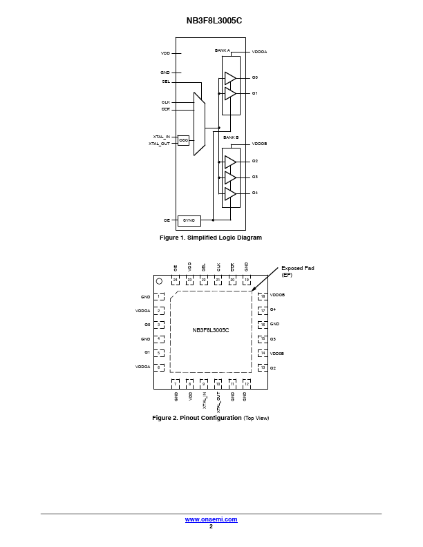
Description The NB3F8L3005C is a 2:1:5 Clock / Data fanout buffer operating on a 3.3 V / 2.5 V Core VDD and two flexible 3.3 V / 2.5 V / 1.8 V / 1.5 V VDDOx supplies which must be equal or less than VDD. A Mux selects between a Crystal input, or a differential/SE Clock / Data inputs. Differential Inputs accept LVPECL, LVDS, HCSL, or SSTL and Single−Ended levels. The MUX control line, SEL selects CLK/CLK, or Crystal input pins per Table 3. The Crystal input is disabled when a Clock input is selected. Output enable pin, OE, synchronously forces a High Impedance state (Hi−Z) when Low per Table 4. Outputs consist of five single−ended LVCMOS outputs. www.onsemi.