NB3N3020
NB3N3020 is LVPECL/LVCMOS Clock Multiplier manufactured by onsemi.
3.3 V, LVPECL/LVCMOS Clock Multiplier
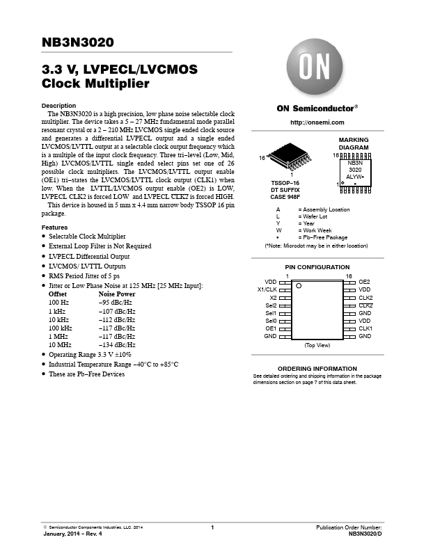
Description The NB3N3020 is a high precision, low phase noise selectable clock multiplier. The device takes a 5
- 27 MHz fundamental mode parallel resonant crystal or a 2
- 210 MHz LVCMOS single ended clock source and generates a differential LVPECL output and a single ended LVCMOS/LVTTL output at a selectable clock output frequency which is a multiple of the input clock frequency. Three tri- level (Low, Mid, High) LVCMOS/LVTTL single ended select pins set one of 26 possible clock multipliers. The LVCMOS/LVTTL output enable (OE1) tri- states the LVCMOS/LVTTL clock output (CLK1) when low. When the LVTTL/LVCMOS output enable (OE2) is LOW, LVPECL CLK2 is forced LOW and LVPECL CLK2 is forced HIGH.
This device is housed in 5 mm x 4.4 mm narrow body TSSOP 16 pin package.
Features
- Selectable Clock Multiplier
- External Loop Filter is Not Required
- LVPECL Differential Output
- LVCMOS/ LVTTL Outputs
- RMS Period Jitter of 5 ps
- Jitter or Low Phase Noise at 125 MHz [25 MHz Input]:
Offset
Noise Power
100 Hz
- 95 d Bc/Hz
1 k Hz
- 107 d Bc/Hz
10 k Hz
- 112 d Bc/Hz
100 k Hz
- 117 d Bc/Hz
1 MHz
- 117 d Bc/Hz
10 MHz
- 134 d Bc/Hz
- Operating Range 3.3 V ±10%
- Industrial Temperature Range
- 40°C to +85°C
- These are Pb- Free Devices...


