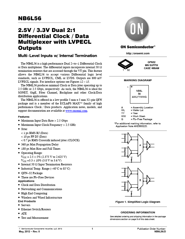
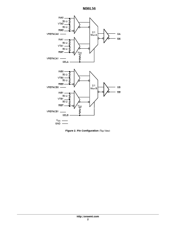
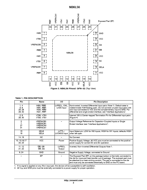
Datasheet4U Logo Datasheet4U.com

NB6L56 - 2.5V / 3.3V Dual 2:1 Differential Clock / Data Multiplexer

Datasheet Summary

Description

Noninverted, Inverted Differential Input pairs (Note 1).

Default state is indeterminate if left floating open.

Features

  • Maximum Input Data Rate > 2.5 Gbps.
  • Maximum Input Clock Frequency > 2.5 GHz.
  • Jitter < 1 ps RMS RJ (Data) < 10 ps PP DJ (Data) < 0.7 ps RMS Crosstalk induced jitter (CLOCK).
  • 360 ps Max Propagation Delay.
  • 180 ps Max Rise and Fall Times.
  • Operating Range: VCC = 2.5 ± 5% (2.375 V to 2.625 V) VCC =3.3 ± 10% (3.0 V to 3.6 V).
  • Internal 50 W Input Termination Resistors.
  • Industrial Temp. Range (.
  • 40°C to 85°C).
  • QFN.

📥 Download Datasheet

Datasheet preview – NB6L56

Datasheet Details

Part number NB6L56
Manufacturer ON Semiconductor
File Size 134.48 KB
Description 2.5V / 3.3V Dual 2:1 Differential Clock / Data Multiplexer
Datasheet download datasheet NB6L56 Datasheet
Additional preview pages of the NB6L56 datasheet.
Other Datasheets by ON Semiconductor

Full PDF Text Transcription

Click to expand full text
NB6L56 2.5V / 3.3V Dual 2:1 Differential Clock / Data Multiplexer with LVPECL Outputs Multi−Level Inputs w/ Internal Termination The NB6L56 is a high performance Dual 2−to−1 Differential Clock or Data multiplexer. The differential inputs incorporate internal 50 W termination resistors that are accessed through the VT pin. This feature allows the NB6L56 to accept various Differential logic level standards, such as LVPECL, CML or LVDS. Outputs are 800 mV LVPECL signals. For interface options see Figures 12 − 15. The NB6L56 produces minimal Clock or Data jitter operating up to 2.5 GHz or 2.5 Gbps, respectively. As such, the NB6L56 is ideal for SONET, GigE, Fiber Channel, Backplane and other Clock/Data distribution applications.
Published: |