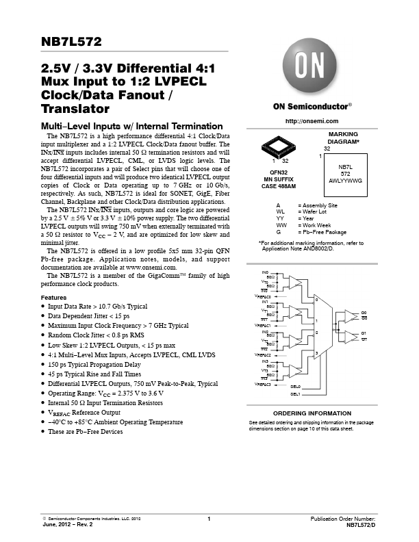
NB7L572 Description
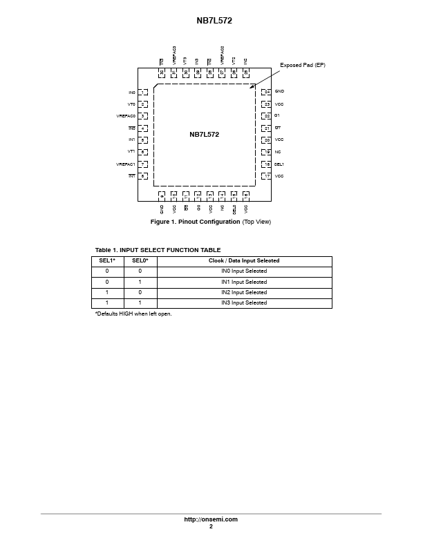
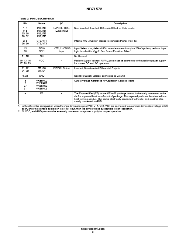
The INx/INx inputs includes internal 50 W termination resistors and will accept differential LVPECL, CML, or LVDS logic levels. The NB7L572 incorporates a pair of Select pins that will choose one of four differential inputs and will produce two identical LVPECL output copies of Clock or Data operating up to 7 GHz or 10 Gb/s, respectively. As such, NB7L572 is ideal for SONET, GigE, Fiber Channel, Backplane and other...
NB7L572 Key Features
- Input Data Rate > 10.7 Gb/s Typical
- Data Dependent Jitter < 15 ps
- Maximum Input Clock Frequency > 7 GHz Typical
- Random Clock Jitter < 0.8 ps RMS
- Low Skew 1:2 LVPECL Outputs, < 15 ps max
- 4:1 Multi-Level Mux Inputs, Accepts LVPECL, CML LVDS
- 150 ps Typical Propagation Delay
- 45 ps Typical Rise and Fall Times
- Differential LVPECL Outputs, 750 mV Peak-to-Peak, Typical
- Operating Range: VCC = 2.375 V to 3.6 V
NB7L572 Applications
- 2 V, and are optimized for low skew and minimal jitter