NCP5183
Features
- Automotive Qualified to AEC Q100
- Voltage Range: up to 600 V
- d V/dt Immunity 50 V/ns
- Gate Drive Supply Range from 9 V to 18 V
- Output Source / Sink Current Capability 4.3 A / 4.3 A
- 3.3 V and 5 V Input Logic patible
- Extended Allowable Negative Bridge Pin Voltage Swing to
- 10 V
Matched Propagation Delays between Both Channels Propagation Delay 120 ns typically Under VCC Lock Out (UVLO) for Both Channels
- Pin to Pin patible with Industry Standards
- These are Pb- free Devices
Typical Application
- Power Supplies for Tele and Data
- Half- Bridge and Full- Bridge Converters
- Push- Pull Converters
- High Voltage Synchronous- Buck Converters
- Motor Controls
- Electric Power Steering
- Class- D Audio Amplifiers
DATA SHEET .onsemi.
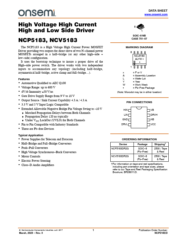
8 1
SOIC- 8 NB CASE 751- 07
MARKING DIAGRAM
NCx5183 ALYW G
1 x
= P or V
= Assembly Location
= Wafer Lot
= Year
= Work Week
= Pb- Free Package
(Note: Microdot may be in either...