NTD5865NL Overview
Key Specifications
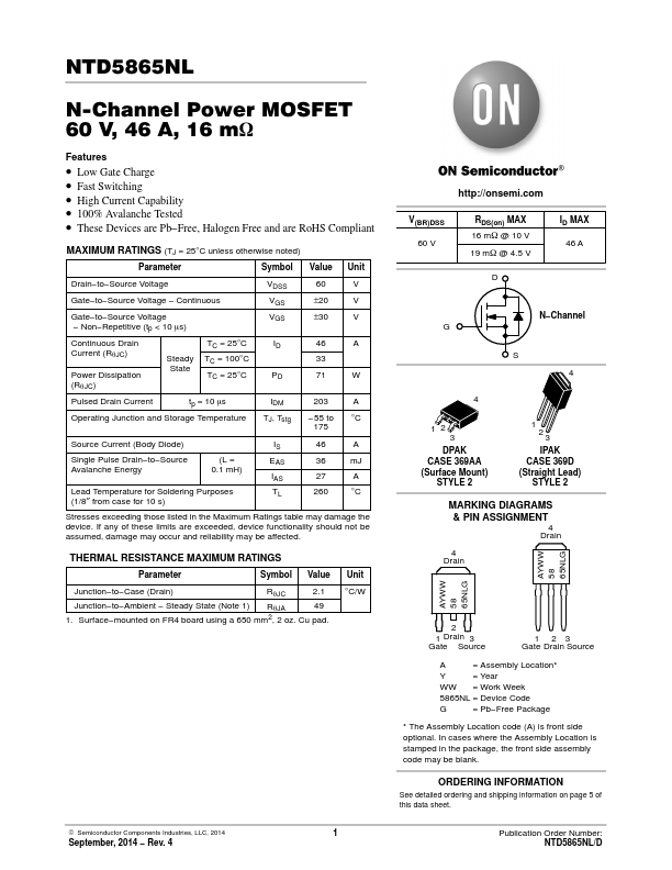
Package: DPAK
Pins: 4
Height: 2.38 mm
Length: 6.73 mm
Key Features
- V(BR)DSS 60 V Value 60 20 30 40 26 PD IDM TJ, Tstg IS (L = 0.1 mH) EAS IAS TL 52 137 -- 55 to 150 40 36 27 260 W A C 4 A mJ A C 3 DPAK CASE 369AA (Surface Mount) STYLE 2 1 2 1 2 Unit V V V A RDS(on) MAX 16 mΩ @ 10 V 19 mΩ @ 4.5 V ID MAX 40 A