NTMFS4941N
NTMFS4941N is Power MOSFET manufactured by onsemi.
Features
30 V, 47 A, Single N- Channel, SO- 8 FL
- -
- -
Low RDS(on) to Minimize Conduction Losses Low Capacitance to Minimize Driver Losses Optimized Gate Charge to Minimize Switching Losses These Devices are Pb- Free, Halogen Free/BFR Free and are Ro HS pliant
.. http://onsemi.
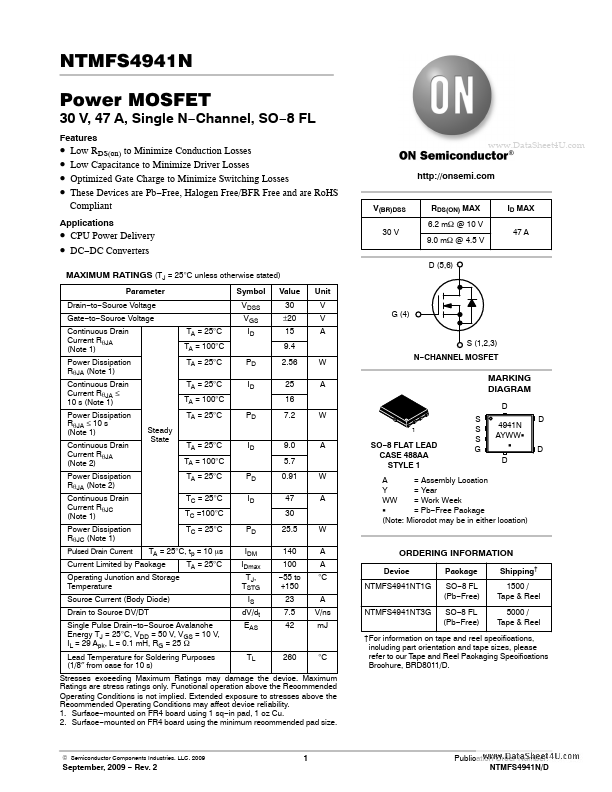
V(BR)DSS 30 V RDS(ON) MAX 6.2 m W @ 10 V 9.0 m W @ 4.5 V D (5,6) ID MAX 47 A
Applications
- CPU Power Delivery
- DC- DC Converters
MAXIMUM RATINGS (TJ = 25°C unless otherwise stated)
Parameter Drain- to- Source Voltage Gate- to- Source Voltage Continuous Drain Current Rq JA (Note 1) Power Dissipation Rq JA (Note 1) Continuous Drain Current Rq JA ≤ 10 s (Note 1) Power Dissipation Rq JA ≤ 10 s (Note 1) Continuous Drain Current Rq JA (Note 2) Power Dissipation Rq JA (Note 2) Continuous Drain Current Rq JC (Note 1) Power Dissipation Rq JC (Note 1)
Pulsed Drain Current
Symbol VDSS VGS TA = 25°C TA = 100°C TA = 25°C TA = 25°C TA = 100°C TA = 25°C PD ID PD ID PD IDM IDmax TJ, TSTG IS d V/dt EAS PD ID ID
Value 30 ±20 15 9.4 2.56 25 16 7.2
Unit V V A S (1,2,3) W A N- CHANNEL MOSFET G (4)
MARKING DIAGRAM
Steady State
TA = 25°C TA = 100°C TA = 25°C TC = 25°C TC =100°C TC = 25°C
9.0 5.7 0.91 47 30 25.5 140 100
- 55 to +150 23 7.5 42
SO- 8 FLAT LEAD CASE 488AA STYLE 1
4941N AYWWG G D
W A A °C A V/ns m J
A = Assembly Location Y = Year WW = Work Week G = Pb- Free Package (Note: Microdot may be in either location)
TA = 25°C, tp = 10 ms TA = 25°C
ORDERING INFORMATION
Device NTMFS4941NT1G NTMFS4941NT3G Package SO- 8 FL (Pb- Free) SO- 8 FL (Pb- Free) Shipping† 1500 / Tape & Reel 5000 / Tape & Reel
Current Limited by Package Operating Junction and Storage Temperature Source Current (Body Diode) Drain to Source DV/DT
Single Pulse Drain- to- Source Avalanche Energy TJ = 25°C, VDD = 50 V, VGS = 10 V, IL = 29 Apk, L = 0.1 m H, RG = 25 W Lead Temperature for Soldering Purposes (1/8″ from case for 10 s)
°C
†For information on tape and reel specifications, including part orientation and...