MMBD6100LT1 Overview
Key Features
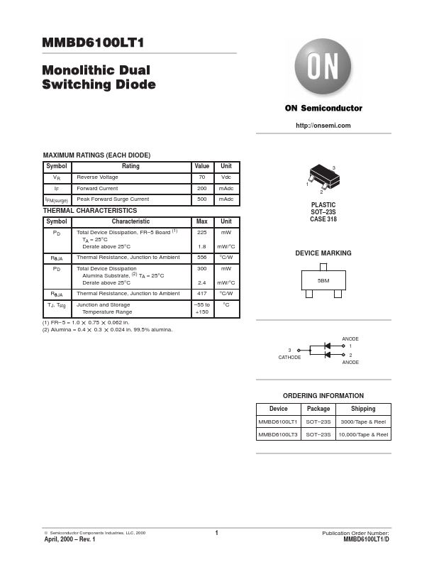
- 23S CASE 318
- 5 Board TA = 25°C Derate above 25°C
| Part Number | Manufacturer | Description |
|---|---|---|
| MMBD6100LT1 | Motorola Semiconductor | Monolithic Dual Switching Diodes |
| MMBD6100 | PanJit Semiconductor | SURFACE MOUNT SWITCHING DIODES |
| MMBD6100 | Formosa MS | SMD Switching Diode |
| MMBD6100W | PanJit Semiconductor | SURFACE MOUNT SWITCHING DIODES |
| MMBD6100 | Power Silicon | SURFACE MOUNT SWITCHING DIODES |