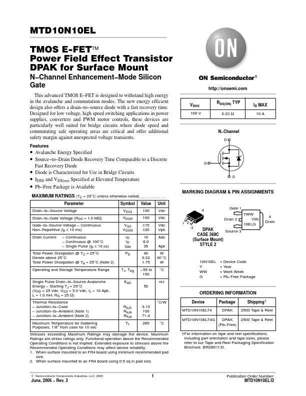
MTD10N10EL Description
MTD10N10EL TMOS E−FET™ Power Field Effect Transistor DPAK for Surface Mount N−Channel Enhancement−Mode Silicon Gate This advanced TMOS E−FET is designed to withstand high energy in the avalanche and mutation modes. The new energy efficient design also offers a drain−to−source diode with a fast recovery time. Designed for low voltage, high speed switching applications in power supplies, converters and PWM motor...
MTD10N10EL Key Features
- Avalanche Energy Specified
- Source-to-Drain Diode Recovery Time parable to a Discrete
- Fast Recovery Diode Diode is Characterized for Use in Bridge Circuits IDSS and VDS(on) Specified at Elevated Temperature
- Continuous Non-Repetitive (tp ≤ 10 ms) Drain Current
- Continuous
- Continuous @ 100°C
- Starting TJ = 25°C (VDD = 25 Vdc, VGS = 5.0 Vdc, IL = 10 Apk, L = 1.0 mH, RG = 25 W) Thermal Resistance
- Junction-to-Case
- Junction-to-Ambient (Note 1)
- Junction-to-Ambient (Note 2) Maximum Temperature for Soldering Purposes, 1/8″ from case for 10 sec